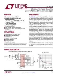
Transcription of LT1720/LT1721 - Dual/Quad, 4.5ns, Single Supply 3V/5V ...
1 LT1720/LT1721117201fc TYPICAL APPLICATION DESCRIPTIONDual/Quad, , SingleSupply 3V/5V Comparatorswith Rail-to-Rail OutputsThe LT 1720/LT1721 are UltraFastTM dual/quad compara -tors optimized for Single Supply operation, with a Supply voltage range of to 6V. The input voltage range extends from 100mV below ground to below the Supply volt-age. Internal hysteresis makes the LT1720/LT1721 easy to use even with slow moving input signals. The rail-to-rail outputs directly interface to TTL and CMOS. Alternatively, the symmetric output drive can be harnessed for analog applications or for easy translation to other Single Supply logic LT1720 is available in three 8-pin packages; three pins per comparator plus power and ground. In addition to SO and MSOP packages, a 3mm 3mm low profi le ( ) dual fi ne pitch leadless package (DFN) is available for space limited applications.
2 The LT1721 is available in the 16-pin SSOP and S packages. The pinouts of the LT1720/LT1721 minimize parasitic effects by placing the most sensitive inputs (inverting) away from the outputs, shielded by the power rails. The LT1720/LT1721 are ideal for systems where small size and low power are to 6V Crystal Oscillator with TTL/CMOS OutputL, LT, LTC and LTM are registered trademarks of Linear Technology Corporation. UltaFast is a trademark of Linear Technology Corporation. All other trademarks are the property of their respective owners. FEATURES APPLICATIONSn High Speed Differential Line Receivern Crystal Oscillator Circuitsn Window Comparatorsn Threshold Detectors/Discriminatorsn Pulse Stretchersn Zero-Crossing Detectorsn High Speed Sampling Circuitsn UltraFast: at 20mV Overdrive 7ns at 5mV Overdriven Low Power: 4mA per Comparator n Optimized for 3V and 5V Operationn Pinout Optimized for High Speed Ease of Usen Input Voltage Range Extends 100mV Below Negative Railn TTL/CMOS Compatible Rail-to-Rail Outputsn Internal Hysteresis with Specifi ed Limitsn Low Dynamic Current Drain.
3 15 A/(V-MHz), Dominated by Load In Most Circuitsn Tiny 3mm 3mm DFN Package (LT1720)Propagation Delay vs Overdrive +C11/2 TO 6V2k620 220 1 MHz TO 10 MHzCRYSTAL (AT-CUT)2k17201 (mV)0 DELAY (ns)305017201 TA0210204087654321025 CVSTEP = 100mVVCC = 5 VCLOAD = 10pFRISING EDGE(tPDLH)FALLING EDGE(tPDHL)LT1720/LT1721217201fc ABSOLUTE MAXIMUM RATINGSS upply Voltage, VCC to GND ..7 VInput Current .. 10mAOutput Current (Continuous) .. 20mAJunction Temperature .. 150 C (DD Package) .. 125 CLead Temperature (Soldering, 10 sec) .. 300 C(Note 1)TOP VIEWDD PACKAGE8-LEAD (3mm s 3mm) PLASTIC DFN56784321+IN A IN A IN B+IN BVCCOUT AOUT BGND9 TJMAX = 125 C, JA = 160 C/WUNDERSIDE METAL INTERNALLY CONNECTED TO GND1234+IN A IN A IN B+IN B8765 VCCOUT AOUT BGNDTOP VIEWMS8 PACKAGE8-LEAD PLASTIC MSOPTJMAX = 150 C, JA = 230 C/WTOP VIEWVCCOUT AOUT BGND+IN A IN A IN B+IN BS8 PACKAGE8-LEAD PLASTIC SO12348765 TJMAX = 150 C, JA = 200 C/W12345678 TOP VIEWGN PACKAGE16-LEAD NARROWPLASTIC SSOPS PACKAGE16-LEAD PLASTIC SO161514131211109 IN A+IN AGNDOUT AOUT BGND+IN B IN B IN D+IN DVCCOUT DOUT CVCC+IN C IN CTJMAX = 150 C, JA = 135 C/W (GN)TJMAX = 150 C, JA = 115 C/W (S) PIN CONFIGURATIONS torage Temperature Range.
4 65 C to 150 C (DD Package) .. 65 C to 125 COperating Temperature Range C Grade .. 0 C to 70 C I Grade .. 40 C to 85 CLT1720/LT1721317201fc ELECTRICAL CHARACTERISTICSSYMBOLPARAMETERCONDITIONS MINTYPMAXUNITSVCCS upply Current (Per Comparator)VCC = 5 VVCC = Mode Voltage Range(Note 2)l +Input Trip Points(Note 3)l Input Trip Points(Note 3)l Offset Voltage(Note 3) Hysteresis Voltage(Note 3) VOS/ TInput Offset Voltage Driftl10 V/ CIBI nput Bias Currentl 60 AIOSI nput Offset ACMRRC ommon Mode Rejection Ratio(Note 4)l5570dBPSRRP ower Supply Rejection Ratio(Note 5)l6580dBAVV oltage Gain(Note 6) VOHO utput High VoltageISOURCE = 4mA, VIN = VTRIP+ + 10mVlVCC Low VoltageISINK = 10mA, VIN = VTRIP DelayVOVERDRIVE = 20mV (Note 7) DelayVOVERDRIVE = 5mV (Notes 7, 8)l71013nsns The l denotes specifi cations that apply over the full operating temperature range, otherwise specifi cations are at TA = 25 C.
5 VCC = 5V, VCM = 1V, COUT = 10pF, VOVERDRIVE = 20mV, unless otherwise specifi ed. ORDER INFORMATIONLEAD FREE FINISHTAPE AND REELPART MARKING*PACKAGE DESCRIPTIONTEMPERATURE RANGELT1720 CDD#PBFLT1720 CDD#TRPBFLAAV8-Lead (3mm 3mm) Plastic DFN0 C to 70 CLT1720 IDD#PBFLT1720 IDD#TRPBFLAAV8-Lead (3mm 3mm) Plastic DFN 40 C to 85 CLT1720 CMS8#PBFLT1720 CMS8#TRPBFLTDS8-Lead Plastic MSOP0 C to 70 CLT1720 IMS8#PBFLT1720 IMS8#TRPBFLTACW8-Lead Plastic MSOP 40 C to 85 CLT1720CS8#PBFLT1720CS8#TRPBF17208-Lead Plastic SO0 C to 70 CLT1720IS8#PBFLT1720IS8#TRPBF1720I8-Lead Plastic SO 40 C to 85 CLT1721 CGN#PBFLT1721 CGN#TRPBF172116-Lead Narrow Plastic SSOP0 C to 70 CLT1721 IGN#PBFLT1721 IGN#TRPBF1721I16-Lead Narrow Plastic SSOP 40 C to 85 CLT1721CS#PBFLT1721CS#TRPBF172116-Lead Plastic SO0 C to 70 CLT1721IS#PBFLT1721IS#TRPBF1721I16-Lead Plastic SO 40 C to 85 CConsult LTC Marketing for parts specifi ed with wider operating temperature ranges.
6 *The temperature grade is identifi ed by a label on the shipping LTC Marketing for information on non-standard lead based fi nish more information on lead free part marking, go to: For more information on tape and reel specifi cations, go to: TYPICAL PERFORMANCE CHARACTERISTICSSUPPLY VOLTAGE (V) AND TRIP POINT VOLTAGE (mV)3210 1 2 +VOSVTRIP 25 CVCM = 1 VTEMPERATURE ( C) 3 VOSAND TRIP POINT VOLTAGE (mV) 113 202 252510017201 G02 5005075125 VTRIP+VOSVTRIP TEMPERATURE ( C) 25050100125 MODE INPUT VOLTAGE (V)VCC = 5 VInput Offset and Trip Voltages vs Supply VoltageInput Offset and Trip Voltages vs TemperatureInput Common Mode Limitsvs TemperatureNote 1: Stresses beyond those listed under Absolute Maximum Ratings may cause permanent damage to the device. Exposure to any Absolute Maximum Rating condition for extended periods may affect device reliability and 2: If one input is within these common mode limits, the other input can go outside the common mode limits and the output will be 3: The LT1720/LT1721 comparators include internal hysteresis.
7 The trip points are the input voltage needed to change the output state in each direction. The offset voltage is defi ned as the average of VTRIP+ and VTRIP , while the hysteresis voltage is the difference of these 4: The common mode rejection ratio is measured with VCC = 5V and is defi ned as the change in offset voltage measured from VCM = to VCM = , divided by 5: The power Supply rejection ratio is measured with VCM = 1V and is defi ned as the change in offset voltage measured from VCC = to VCC = 6V, divided by ELECTRICAL CHARACTERISTICS The l denotes specifi cations that apply over the full operating temperature range, otherwise specifi cations are at TA = 25 C.
8 VCC = 5V, VCM = 1V, COUT = 10pF, VOVERDRIVE = 20mV, unless otherwise specifi ed. SYMBOLPARAMETERCONDITIONSMINTYPMAXUNITS tPDDifferential Propagation Delay(Note 9) Between Delay Skew(Note 10) Between Rise Time10% to 90% Fall Time90% to 10% Timing JitterVIN = (6dBm), ZIN = 50 tPDLHVCM = 2V, f = 20 MHz tPDHL1511psRMSpsRMSfMAXM aximum Toggle FrequencyVOVERDRIVE = 50mV, VCC = 3 VVOVERDRIVE = 50mV, VCC = 6: Because of internal hysteresis, there is no small-signal region in which to measure gain. Proper operation of internal circuity is ensured by measuring VOH and VOL with only 10mV of 7: Propagation delay measurements made with 100mV steps. Overdrive is measured relative to VTRIP .Note 8: tPD cannot be measured in automatic handling equipment with low values of overdrive. The LT1720/LT1721 are 100% tested with a 100mV step and 20mV overdrive.
9 Correlation tests have shown that tPD limits can be guaranteed with this test, if additional DC tests are performed to guarantee that all internal bias conditions are correct. Note 9: Differential propagation delay is defi ned as the larger of the two: tPDLH = tPDLH(MAX) tPDLH(MIN) tPDHL = tPDHL(MAX) tPDHL(MIN)where (MAX) and (MIN) denote the maximum and minimum values of a given measurement across the different comparator 10: Propagation Delay Skew is defi ned as: tSKEW = |tPDLH tPDHL|LT1720/LT1721517201fcTYPICAL PERFORMANCE CHARACTERISTICSDIFFERENTIAL INPUT VOLTAGE (V) 5 7 INPUT CURRENT ( A) 6 4 3 21234217201 G04 5 4 3 2 105 10125 CVCC = 5 VTEMPERATURE ( C) 50 QUIESCENT Supply CURRENT PER COMPARATOR (mA) = 5 VVCC = 3 VSUPPLY VOLTAGE (V)00 Supply CURRENT PER COMPARATOR (mA)4724517201 G0632165136725 C125 C 55 COUTPUT LOAD CAPACITANCE (pF)0 DELAY (ns)305017201 G07102040987654321025 CVSTEP = 100mVOVERDRIVE = 20mVVCC = 5 VRISING EDGE(tPDLH)FALLING EDGE(tPDHL)TEMPERATURE ( C) 50 PROPAGATION DELAY (ns) = 3 VVCC = 3 VVCC = 5 VVCC = 5 VtPDLHVCM = 1 VVSTEP = 100mVCLOAD = 10pFOVERDRIVE = 5mVOVERDRIVE = 20mVSUPPLY VOLTAGE (V) (ns) EDGE(tPDLH)FALLING EDGE(tPDHL)25 CVSTEP = 100mVOVERDRIVE = 20mVCLOAD = 10pFOUTPUT SINK CURRENT (mA)0 OUTPUT VOLTAGE (V)
10 C25 C125 CVCC = = 5 VVCM = 1 VVIN = 15mV 55 COUTPUT SOURCE CURRENT (mA)0 OUTPUT VOLTAGE RELATIVE TO VCC (V) G11 C 55 C25 C25 CVCC = = 5 VVCM = 1 VVIN = 15mVFREQUENCY (MHz)0781030NO LOAD17201 G1265102040439 Supply CURRENT PER COMPARATOR (mA)25 CVCC = 5 VCLOAD = 20pFPropagation Delayvs Load CapacitancePropagation Delay vs TemperaturePropagation Delayvs Supply VoltageOutput Low Voltage vs Load CurrentOutput High Voltagevs Load CurrentSupply Current vs FrequencyInput Current vs Differential Input VoltageQuiescent Supply Currentvs TemperatureQuiescent Supply Currentvs Supply VoltageLT1720/LT1721617201fc PIN FUNCTIONSLT1720+IN A (Pin 1): Noninverting Input of Comparator A. IN A (Pin 2): Inverting Input of Comparator A. IN B (Pin 3): Inverting Input of Comparator B.+IN B (Pin 4): Noninverting Input of Comparator (Pin 5): B (Pin 6): Output of Comparator A (Pin 7): Output of Comparator (Pin 8): Positive Supply IN A (Pin 1): Inverting Input of Comparator A.
