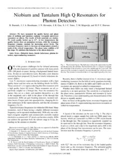
Transcription of IEEE TRANSACTIONS ON APPLIED ... - UMD Physics
1 This article has been accepted for inclusion in a future issue of this journal. Content is final as presented, with the exception of TRANSACTIONS ON APPLIED SUPERCONDUCTIVITY1 Superposition of Inductive and Capacitive Couplingin Superconducting LC ResonatorsSergiy Gladchenko, Moe Khalil, C. J. Lobb, F. C. Wellstood, and Kevin D. OsbornAbstract We present an experimental investigation of lumped-element superconducting LC resonators designed to provide dif-ferent types of coupling to a transmission line. We have designedfour resonator geometries including dipole and quadrupole con-figured inductors connected in parallel with low-loss dielec-tric parallel-plate capacitors. The design of the resonator allowsa change in the symmetry of the inductor or grounding of the ca-pacitor to create LC resonators with: 1) inductive coupling, 2) ca-pacitive coupling, 3) both types of coupling, or 4) greatly reducedcoupling.
2 We measured all four designs at a temperature of 30 mKat different values of power. We compare the extracted data fromthe four resonator types and find that both capacitive and induc-tive coupling can be included and that when nominally turned off,the coupling is greatly reduced from only minor changes in the cir-cuit design. We also find a variation in the measured loss tangentof less than a few percent between the designs over a large rangeof internal quality factors, which are created by using as anonlinear lossy element within the Terms Dielectric losses, electromagnetic coupling, super-conducting INTRODUCTIONSUPERCONDUCTING resonators with parallel plate(lumped element) capacitors are present in a numberof devices including phase qubits [1], amorphous dielectricresonators [2], [3], and Josephson bifurcation amplifiers [4]. Bydesign, they are compact and lack harmonic modes, and with alow-loss dielectric they can also achieve a high internal-qualityfactor at milli-Kelvin temperatures and low photon numbers[2], [3].
3 The resonant coupling for phase qubits has utilized both ca-pacitive [4] and inductive [5] types of coupling. To change fromone type of coupling to the other the drive line geometry waschanged. However, in principle the coupling could be changedby changing the design of the qubit, while leaving the drive this paper we report on LC resonators, where the designof the resonator is changed to realize different coupling inductive and capacitive coupling are independently addedManuscript received August 02, 2010; accepted October 12, 2010. This re-search was performed at the Laboratory for Physical Sciences. The work of Lobb was supported by Gladchenko and K. D. Osborn are with the Laboratory for Physical Sci-ences, College Park, MD 20740 USA (e-mail: S. Khalil is with the Department of Physics , University of Maryland, Col-lege Park, MD 20740 J.)
4 Lobb and F. C. Wellstood are with the Joint Quantum Institute and theCenter for Nanophysics and Advanced Materials, Department of Physics , Uni-versity of Maryland, College Park, MD 20740 Object Identifier 1. Lump elements schematic diagram of left off with a small change in the resonator design, while thetransmission line is left a result, we superimpose both the inductive and capacitivecoupling in one design, nominally leave the coupling off in an-other design, and include either capacitive or inductive couplingin the remaining 2 designs. This creates a wide range of cou-pling magnitudes or external quality factors. The resonators useadielectric in the capacitor, which has a power dependentloss at low temperatures and allows us to create a wide rangeof internal quality factors. Since the loss of theshould beindependent of the coupling type, we are able to check the con-sistency of the circuit model between resonators with differentexternal quality factors and coupling types, over a range of in-ternal quality DEVICEDESCRIPTION ANDFITTINGMODELFig.
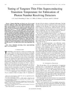
5 1. shows a schematic of a resonator with inductor L andcapacitorcoupled to an input and output transmission transmission lines carry waves traveling to the right withinput amplitudeand output amplitude. Coupling tothe LC resonator is achieved through a capacitoror a mutualinductance M. Four different resonator designs were tested withdifferent types of first consider a resonator with capacitive coupling. InFig. 1 the capacitorrepresents the capacitive coupling be-tween the center conductor of the resonator and one side of thecapacitor. This capacitor allows energy to be coupled from theinput transmission line to the LC resonator. On the other sideof the LC resonator is a grounding wire (represented by a wirebetween two circular terminals in Fig. 1). As shown, this cir-cuit shows capacitive coupling because current will be drivenacross the LC circuit on resonance.
6 If however the groundingwire is not connected, no current can flow through the capacitorand the resonator is capacitively decoupled. In our real de-vice, there will be stray capacitances (not shown) which allowsome current to flow through, but the device is nominallycapacitively decoupled. The other coupling type is inductive. In1051-8223/$ 2010 IEEEThis article has been accepted for inclusion in a future issue of this journal. Content is final as presented, with the exception of TRANSACTIONS ON APPLIED SUPERCONDUCTIVITYFig. 2. Optical microscope images of resonator (light grey is metallization,black is sapphire substrate, dark grey is ). White squares in the (a) imageindicate position of elements defining the type of coupling. Top square repre-sents resonator grounding, bottom square show inductor. Images (b) (e) demon-strated possible variation of these elements for different resonators.
7 (b) groundedresonator (top plate of capacitor connected to the grounded environment); (c)non-grounded resonator; (d) quadruple shaped loop of inductor; and (e) dipoleshaped loop of 1,couples magnetic flux into the inductor L, throughmutual inductance M such that. In our resonatorswe have two types of inductive coupling. In one case, the in-ductor is configured as a simple loop or dipole and the value ofM is finite and appreciable. In the second case, L is configuredas a first order gradiometer (quadrupole), such that the couplingM is nominally micrograph of a complete resonator with a quadrupole coilis shown in Fig. 2(a). All four resonator designs have the samecapacitor layout, with a top plate size of 20by 325,which is intentionally small in one dimension to avoid trappingof magnetic vortices. The plates of the capacitor are connectedto an inductor.
8 A coplanar waveguide passes by the capacitorwith a ground plane on either side of center conductor, which islabeled with arrows. The inductor and capacitor are embeddedwithin a rectangular hole in the ground plane (not shown) of 2(a) shows a resonator with the top plate of the capacitorconnected to ground. This connection is made in the region inthe upper dashed box, and Fig. 2(b) shows a detailed view. Forresonators where the capacitor is nominally decoupled, this con-nection is not present, as shown in Fig. 2(c). The lower dashedbox in Fig. 2(a) shows a quadrupole inductor, and a separateview is shown in Fig. 2(d). This inductor has no nominal induc-tive coupling. In the inductively coupled designs this inductoris replaced with a simple meander loop or dipole inductor, asshown in Fig. 2(e).The fabricated resonators realize all four possible combina-tions of these coupling types: capacitive coupling (C), inductivecoupling (L), inductively and capacitive coupling (LC), anda nominally uncoupled resonator which has a low value ofresidual devices were fabricated starting from an Al film that wassputtered on a sapphire substrate.
9 We used optical lithographyand a wet etch to pattern the base layer. An amorphous dielectriclayer of SiNx was deposited on the base layer at 300usingplasma-enhanced chemical vapor deposition (PECVD). Next areactive ion etch (RIE) was used to open a via through the di-electric. The upper wiring layer was then added by first usingan ion mill to clean the exposed Al surface. Finally, a second Allayer was sputtered and then patterned in a similar manner asthe base MEASUREMENTTECHNIQUEThe resonators were mounted on a dilution refrigerator,cooled to 30 mK, and the complex transmission amplitudewas measured using a vector network analyser. Toreduce thermally generated noise from reaching the resonator,the input microwave line was attenuated by 20 dB at both 1 Kand 30 mK stages and the output line has two Pamtech circula-tors at the 30 mK stage.
10 These steps allow the thermal photonbackground below a single photon within the bandwidth of theresonator. The transmitted signal is amplified with a HEMT amplifier at 4 K and a low noise amplifier at room measured transmission amplitude versus frequency wasfit to a model function derived from Fig. 1. For weak couplingwe can make the approximationsand wefind(1)whereis APPLIED microwave frequency,is the resonancefrequency,is the total quality factor,is the externalquality factor andis a constant nearly equal to lowest order,(2)and the internal quality factor(3)is calculated from(4)Since here we will only attribute internal loss in the resonator todielectric loss in the resonator capacitor, we can write(5)where C is the real part of capacitance andis the dielectricloss tangent. This gives an internal quality factor that is inverselyproportional to the internal dielectric EXPERIMENTS ANDDISCUSSIONThe experimentally measured complex transmission ampli-tude has been fit with model function (1) using,,, andas fitting parameters.