Transcription of 860 IEEE TRANSACTIONS ON APPLIED …
1 860 ieee TRANSACTIONS ON APPLIED SUPERCONDUCTIVITY, VOL. 15, NO. 2, JUNE 2005 Fabrication and Characterization of SuperconductingCircuit QED Devices for Quantum ComputationLuigi Frunzio, Andreas Wallraff, David Schuster, Johannes Majer, and Robert SchoelkopfAbstract We present fabrication and characterization proce-dures of devices for circuit quantum electrodynamics (cQED).We have made 3-GHz cavities with quality factors in the range104 106, which allow access to the strong coupling regime ofcQED. The cavities are transmission line resonators made byphotolithography. They are coupled to the input and output portsvia gap capacitors. An Al-based Cooper pair box is made bye-beam lithography and Dolan bridge double-angle evaporationin superconducting resonators with high quality factor.
2 An impor-tant issue is to characterize the quality factor of the present an RF-characterization of superconducting resonatorsas a function of temperature and magnetic field. We have realizeddifferent versions of the system with different box-cavity couplingsby using different dielectrics and by changing the box , the cQED approach can be used as a diagnostic tool ofqubit internal Terms Distributed parameter circuits, Q factor, scat-tering parameters measurement, superconducting cavity INTRODUCTIONWE have recently demonstrated that a superconductingquantum two-level system can be strongly coupled to asingle microwave photon [1], [2]. The strong coupling betweena quantum solid state circuit and an individual photon, analo-gous to atomic cavity quantum electrodynamics (CQED) [3],has previously been envisaged by many authors, see [4] and ref-erences therein.
3 Our circuit quantum electrodynamics architec-ture [4], in which a superconducting charge qubit, the Cooperpair box (CPB) [5], is coupled strongly to a coplanar trans-mission line resonator, has great prospects both for performingquantum optics experiments [6] in solids and for realizing ele-ments for quantum information processing [7] with supercon-ducting circuits [8] [14] and also for other architectures [15],[16].In developing these qubit-resonator systems, one key ingre-dient is to design and realize transmission line resonators withhigh internal quality factor,, and with resonant frequency,, in the 5 15 GHz range to match the other energy scales ofour device, and to be in the quantum regimeatmK. On the other hand, the resonator is loadedwith input and output capacitances and we need a loaded qualityManuscript received October 4, 2004.
4 This work was supported in part bythe National Security Agency (NSA) and Advanced Research and DevelopmentActivity (ARDA) under Army Research Office (ARO) Contract DAAD19-02-1-0045, the NSF ITR Program under Grant DMR-0325580, the NSF under GrantDMR-0342157, the David and Lucile Packard Foundation, and the W. M. authors are with the Department of APPLIED Physics, Yale University,New Haven, CT 06520 USA (e-mail: Object Identifier order to obtain reasonably fast rate of mea-surement, fabricating the transmission line resonator, we opted for acoplanar waveguide (CPW) for many different reasons. First, aCPW has a simple layer structure with no need for depositedinsulators. Second, it has a balanced structure with a relativelyeasy planar connection to the CPB. Third, a CPW has athatis relatively insensitive to kinetic inductance and dominated bygeometrical distributed inductance.)
5 Last but not the least, CPW-based structures, made by Al thin film deposited on sapphire,have been recently shown [17] to allow very high s (order of).We decided to fabricate on passivated Si wafers because thisis the substrate on which we had previously developed the qubitfabrication. We also decided to try as material for the resonatorsboth Al, for easy compatibility with the qubit process, and Nb,because its higher critical temperature allows testing of res-onators at higher Section II, we present design consideration for devices forcircuit quantum electrodynamics (cQED). We will show thatwe can engineerwith different coupling of the resonator tothe input and output ports and that the internal losses can bemade negligible at the designed[1], [2]. Section III intro-duces the fabrication procedures for both the resonator and theCPB.
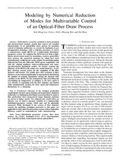
6 Sections IV VI present an RF-characterization of the su-perconducting transmission line resonators versus temperatureand magnetic CIRCUITDESIGNA picture of ammchip containing a 3-GHz super-conducting Nb CPW resonator is shown in Fig. 1(a). The lengthof the meandering resonator ismm. The center con-ductor is 10m wide, separated from the lateral ground planesextending to the edges of the chip by a 5m gap, resulting ina wave impedance of the coplanar waveguide oftomatch the impedance of conventional microwave capacitance per unit length ismwhichgives a total resonator capacitance resonator is coupled by identical capacitors at each end (seesolid line square in Fig. 1(a)) to an input and output feed line,fanning out to the edge of the chip and keeping the impedanceconstant. In Fig.
7 1(b) and (1d) are shown micrographs of twoof the coupling capacitors with different geometries. The one inFig. 1(b) consists of two 100-m long and 4-m wide fingersseparated by a 2-m gap. It has a capacitance,,larger than that in Fig. 1(d), which has a simpler geometry witha4-m gap $ 2005 IEEEFRUNZIOet al.: FABRICATION AND CHARACTERIZATION OF cQED DEVICES861 Fig. 1. Picture of a device for circuit QED. (a) The 3 GHz superconductingcoplanar waveguide resonator is fabricated using optical lithography. The lengthof the meandering resonator isl=24mm. The center conductor is 10 mwide, separated from the lateral ground planes extending to the edges of thechip by a 5 m gap. The resonator is coupled by identical capacitors at eachend (solid line squares) to input and output ports. (b) Micrograph of a couplingcapacitance with two 100 m long and 4 m widefingers separated by a 2 mgap.
8 (c) Scanning electron micrograph of a Cooper pair box fabricated onto thesilicon substrate into the gap between the center conductor (top) and the groundplane(bottom) in the center of a resonator (dashed line square) using electronbeam lithography and double angle evaporation of aluminum. (d) Micrographof a coupling capacitance with a 4 m capacitive coupling to the input and output lines, togetherwith the loading impedance,, are very important indetermining the loaded quality factor,defined by(1)where the external quality factor is(2)with(3)There are two possible regimes for the resonator. It can beundercoupled whenis small (like) and then. This is the regime in which it is possible to , the resonator can be overcoupled whenis large(like) and then. It is then possible to engineertheto obtain fast measurement withmuch larger than thequbit decay rates [1], [2].
9 In Fig. 1(c) an electron micrograph of a Cooper pair box isshown. The CPB consists of a 7-m long and 200-nm wide su-perconducting island parallel to the center conductor which iscoupled via twonmsize Josephson tunnel junc-tions to a much larger superconducting reservoir. The CPB isfabricated onto the silicon substrate [see dashed line square inFig. 1(a)] in the gap between the center conductor (top) and theground plane (bottom) at an antinode of the electricfield in theresonator. The Josephson junctions are formed at the overlapbetween the island and thefingers extending from the reser-voir, which is capacitively coupled to the ground plane. TheCPB is a two-state system described by the Hamiltonianwhereis the electrostatic energy andis the Josephson energy. The overallenergy scales of these terms, the charging energyand theJosephson energy, can be readily engineered duringthe fabrication by the choice of the total box capacitance andresistance respectively, and then further tunedin situby elec-trical means.
10 Aflux bias, APPLIED with an externalcoil to the loop of the box, controls. We have demonstratedthat changing the length of the CPB island and its distance tothe center conductor and changing the dielectrics (removing thepassivation step of the Si substrate), we can obtain stronger cou-plings of qubit and resonator as predicted by simple electrostaticcalculations of the DEVICEFABRICATIONThe pattern of 36 different Nb resonators is generatedexposing a bilayer photoresist (600 nm LOR5A and ) through a mask with traditional UV a 200-nm thick Nbfilm is dc magnetron sputtered in Arat Pa with a rate of 1 nm/s in an UHV system with a basepressure of 20. The substrate is a300-m thick p-doped(Boron) (100) oriented Si wafer with resistivitycmpreviously passivated by thermal wet oxidation with a 470-nmthick layer of.