Transcription of IEEE TRANSACTIONS ON APPLIED SUPERCONDUCTIVITY, …
1 ieee TRANSACTIONS ON APPLIED superconductivity , VOL. 17, NO. 2, JUNE 2007263 Niobium and Tantalum High Q Resonators forPhoton DetectorsR. Barends, J. J. A. Baselmans, J. N. Hovenier, J. R. Gao, S. J. C. Yates, T. M. Klapwijk, and H. F. C. HoeversAbstract We have measured the quality factors and phasenoise of niobium and tantalum coplanar waveguide microwaveresonators on silicon. The results of both materials are reach quality factors up to105. At low temperatures thequality factors show an anomalous increase, while the resonancefrequency remains constant for increasing power levels.
2 Theresonance frequency starts to decrease at temperatures around atenth of the critical temperature. The phase noise exhibits a 1/flike slope. We attribute this behavior to the silicon Terms Dielectric losses, kinetic inductance, photon de-tection, superconducting INTRODUCTIONONE of the greatest challenges for far infrared astronomyis the development of sensitive cameras with many pixels(100100 pixels or more), having a background limited sensi-tivity. To date no such detector exists. Recently a new detectorconcept has been proposed [1], based on kinetic inductance de-tectors (KIDs).Lowmicrowave superconducting resonators with a highquality factor and low noise are the building blocks for consist ofsuperconducting thin film resonators witha high quality factor (Q factor).
3 These resonators are all ca-pacitively coupled to a through line. Near the resonance fre-quency they act as a short, and manifest themselves as a dipin the magnitude and a shift in the phase of the through linetransmission. KIDs are pair breaking detectors; incident radi-ation breaks Cooper pairs into quasiparticles, changing the ki-netic inductance of the superconductor, and thus the resonancefrequency [2], [3].Typical resonance frequencies lie within the GHz band. Manyresonators, each of them having a slightly different resonancefrequency, can be operated simultaneously. With only one wide-band cryogenic amplifier and commercially available readoutelectronics a camera withpixels can become a reality.
4 KIDscan address the spectrum from the submm range to X-ray, de-pending on the antenna or received August 23, 2006. This work was supported by RadioNet(EU) under contract no. Barends, J. N. Hovenier, and T. M. Klapwijk are with the Kavli Instituteof NanoScience, Faculty of APPLIED Sciences, Delft University of Technology,Lorentzweg 1, 2628 CJ Delft, The J. A. Baselmans, S. J. C. Yates, and H. F. C. Hoevers are with the SRONN etherlands Institute for Space Research, Sorbonnelaan 2, 3584 CA Utrecht,The R. Gao is with the Kavli Institute of NanoScience, Faculty of AppliedSciences, Delft University of Technology, Lorentzweg 1, 2628 CJ Delft, TheNetherlands, and also with the SRON Netherlands Institute for Space Research,Sorbonnelaan 2, 3584 CA Utrecht, The Object Identifier 1.
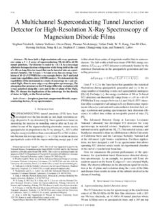
5 The resonator layout. The light areas indicate the superconducting filmand the dark areas the substrate. The transmission line is a coplanar waveguide,the central line of the resonator is 3 mwide, and the gaps are 2 mwide. Theopen end of the resonator is coupled to the main through line, which runs acrossthe chip. The resonator is meandered due to its long length (typically a few mm).Recently, there is further interest in lowmicrowave super-conducting resonators for the field of cavity quantum electrody-namics (CQED) [5]. Both in the KIDs and CQED case lowresonators are operated at subkelvin these KIDs can truly reach a background limitedsensitivity is an open question.
6 The sensitivity is a function ofthe phase noise, quasiparticle lifetime and resonator Q factor[4]. Therefore a clear understanding and characterization of thedevice is urgently , we focus on the quality factor, resonance frequency andphase noise of lowsuperconducting microwave resonators atsubkelvin EXPERIMENTA layout of the structure can be seen in Fig. 1. The chip isplaced inside a copper sample box with two SMA panel con-nectors, which are connected via SMA to CPW circuit boardsto the through line. The resonator is capacitively coupled viaits open end to the through line. Near the resonance frequencyit acts as a short, and a dip in the magnitude and a shift in thephase of the through line transmission can be seen.
7 The trans-mission near the resonance frequency is given by(1)withthe size of the resonance dip,the loaded qualityfactor andthe resonance frequency. The unloaded qualityfactor can be extracted from the transmission since1051-8223/$ 2007 IEEE264 ieee TRANSACTIONS ON APPLIED superconductivity , VOL. 17, NO. 2, JUNE 2007and, withthe cou-pling quality factor andthe unloaded quality optimal materials for KIDs are still a subject of research,as low losses, a long quasiparticle lifetime, the cryogenic systemto be used and KID-antenna coupling schemes are aspects to beconsidered. As superconductors niobium, due to its relativelylarge gap and availability, and tantalum, for its quasiparticlelifetime, are chosen.
8 The niobiumfilm is deposited using DCsputter deposition and has a thickness of 100 nm, a criticaltemperature of K and a residual resistivity ratio (RRR)of 4. Prior to 100 nm tantalum deposition a 5 nm niobiumseed layer was sputtered to promote growth of the tantalumalpha phase [6]. The critical temperature is K, and theRRR is Thefilms are deposited on the native oxide of a[100] oriented silicon substrate having a resistivity in excessof 1and a thickness of 300. Patterning is doneusing dry etching and e-beam lithography for the niobiumand optical lithography for the tantalumfilm.
9 Bothfilms arein the dirty limit; the electron mean free path is smaller thanthe coherence length ().The sample box is mounted on a He-3 sorption cooler in acryostat. Aluminum SMA cables carry the signal from and tothe K cold plate, where a wideband low noise InP MMIC amplifier with a noise temperature of 4 K is mounted. Stainlesssteel SMA cables are used from the cold plate to room temper-ature. A room temperature amplifier is used for extra amplifi-cation. Only semi-rigid and phase stableflexible SMA cablesare used in the setup. For determining the Q factor and reso-nance frequency we measure the forward transmissionwitha Rohde & Schwarz ZVM vector network phase noise is obtained using a homodyne detectionscheme.
10 The on or off resonance signal is generated by thesignal generator. The signal is split with one part travelingthrough the cryostat and KID chip and being mixed with theother part in an IQ mixer. The I and Q channels are sampledwith a 2 channel fast ADC card. A 2 channel variable attenuatoris used to control both the power level at the chip and the powerlevel at the IQ mixer RF input. Hence the magnitude and phaseof the transmitted signal,and, canbe monitored in time. Calculating the power spectral densitygives the magnitude and phase RESULTSWe have measured the Q factor, frequency and phase noiseof a niobium and tantalum resonator.