Transcription of IS32LT3954 - ISSI
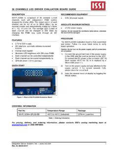
1 IS32LT3954 Integrated Silicon Solution, Inc. 1 Rev. 0B, 11/14/2017 CONSTANT-CURRENT 3-AMPERE PWM DIMMABLE BUCK REGULATOR LED DRIVER WITH FAULT REPORTING Preliminary Information January 2018 GENERAL DESCRIPTION The IS32LT3954 is a DC-to-DC switching converter, which integrate an N-channel MOSFET to operate in a buck configuration. The device supply a wide input voltage between and 40V and provides a constant current of up to 3A for driving a single LED or multiple series connected LEDs. The external resistor, RSET, is used to adjust LED output current, which allowing the output voltage to be automatically adjusted for a variety of LED configurations.
2 The IS32LT3954 operates in a fixed frequency mode during switching. There is an external resistor connected between the VCC and TON pins used to configure the on-time (switching frequency). The switching frequency is dithered for spread spectrum feature to spread the electromagnetic emitting energy into a wider frequency band. It is helpful to optimize the EMI performance. A logic input PWM signal to the enable (EN) pin is applied to adjust the LED current. The brightness of LED is proportional to the duty cycle of the PWM signal. True average output current operation is achieved with fast transient response by using cycle-by-cycle, controlled on-time method.
3 IS32LT3954 is available in an SOP-8-EP package with an exposed pad for enhanced thermal dissipation. It operates from to 40V over the temperature range of -40 C to +125 C. FEATURES Wide input voltage supply from to 40V True average output current control 3A maximum output over operating temperature range Cycle-by-cycle current limit Integrated high-side MOSFET switch Dimming via direct logic input or power supply voltage Internal control loop compensation Under-voltage lockout (UVLO) and thermal shutdown protection 2 A low power shutdown Spread spectrum to optimize EMI Robust fault protection and reporting function.
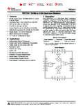
4 - Pin-to-GND short - Component open/short faults - Adjacent pin-to-pin short - LED open/short AEC-Q100 qualification in progress applications Automotive and avionic lighting Dimmable interior lights Daytime running lights Turn/stop lights Front and rear fog lights Map light TYPICAL APPLICATION CIRCUIT Figure 1 Typical Application Circuit IS32LT3954 Integrated Silicon Solution, Inc. 2 Rev. 0B, 11/14/2017 PIN CONFIGURATION Package Pin Configuration (Top View) SOP-8-EP PIN DESCRIPTION No. Pin Description 1 VCC Power supply input. Connect a bypass capacitor CIN to ground.
5 The path from CIN to GND and VCC pins should be as short as possible. 2 TON On-time setting. Connect a resister from this pin to VCC pin to set the regulator controlled on-time. 3 EN/PWM Logic input for enable and PWM dimming. Pull up above to enable and below to disable. Input a 100Hz~20kHz PWM signal to dim the LED brightness. 4 FB Drive output current sense feedback. Set the output current by connecting a resister from this pin to the ground. 5 FAULTB Diagnostic pin. Active low to indicate fault conditions. 6 GND Ground. 7 BOOT Internal MOSFET gate driver bootstrap.
6 Connect a F X7R ceramic capacitor from this pin to LX pin. 8 LX Internal high-side MOSFET switch output. Connect this pin to the inductor and Schottky diode. Thermal Pad Connect to GND. IS32LT3954 Integrated Silicon Solution, Inc. 3 Rev. 0B, 11/14/2017 ORDERING INFORMATION Automotive Range: -40 C to +125 C Order Part No. Package QTY/Reel IS32LT3954 -GRLA3-TR SOP-8-EP, Lead-free 2500 Copyright 2018 Integrated Silicon Solution, Inc. All rights reserved. ISSI reserves the right to make changes to this specification and its products at any time without notice. ISSI assumes no liability arising out of the application or use of any information, products or services described herein.
7 Customers are advised to obtain the latest version of this device specification before relying on any published information and before placing orders for products. Integrated Silicon Solution, Inc. does not recommend the use of any of its products in life support applications where the failure or malfunction of the product can reasonably be expected to cause failure of the life support system or to significantly affect its safety or effectiveness. Products are not authorized for use in such applications unless Integrated Silicon Solution, Inc. receives written assurance to its satisfaction, that: a.) the risk of injury or damage has been minimized; b.
8 The user assume all such risks; and c.) potential liability of Integrated Silicon Solution, Inc is adequately protected under the circumstancesIS32LT3954 Integrated Silicon Solution, Inc. 4 Rev. 0B, 11/14/2017 ABSOLUTE MAXIMUM RATINGS Input voltage, VCC ~ +44V Bootstrap drive voltage, VBOOT ~ VCC +6V Switching voltage, VLX ~ VCC + EN/PWM, TON and FAULTB voltage, VEN/PWM, VTON and ~ VCC + Current sense voltage, VFB ~ Power dissipation, PD(MAX)
9 Operating temperature, TA=TJ -40 C ~ +125 C Storage temperature, TST -65 C ~ +150 C Junction temperature, TJMAX +150 C Junction Package thermal resistance, junction to ambient (4 layer standard test PCB based on JEDEC standard)
10 , JA C/W Package thermal resistance, junction to thermal PAD (4 layer standard test PCB based on JEDEC standard), JP C/W ESD (HBM) ESD (CDM) 2kV 1kV Note: Stresses beyond those listed under Absolute Maximum Ratings may cause permanent damage to the device. These are stress ratings only and functional operation of the device at these or any other condition beyond those indicated in the operational sections of the specifications is not implied. Exposure to absolute maximum rating conditions for extended periods may affect device reliability. ELECTRICAL CHARACTERISTICS VCC= 24V, TJ=TA= -40 C ~ +125 C, Typical values are at TJ = 25 C.