Transcription of Ground Isolation Amplifier - Rohm
1 Product structure Silicon monolithic integrated circuit This product has no designed protection against radioactive rays 1/ 12 TSZ02201-0C2C0EZ00390-1-2 2015 ROHM Co., Ltd. All rights reserved. TSZ22111 14 001 Ground Isolation Amplifier BA3121F General Description BA3121F is a Ground Isolation Amplifier developed for car audio applications. This IC efficiently eliminates problems caused by wiring resistance and removes noise generated by other electrical devices used in automobiles. The external capacitor values required for this IC are so small that it allows for compact and reliable set design.
2 Features Large Capacitors not Required High Common-mode Rejection Ratio Low Noise Low Distortion Two Channels Applications Car audio systems Key Specifications Power Supply Voltage Range: 4V to 18V Quiescent Current: (Typ) High Common-mode Rejection Ratio(1kHz): 57dB (Typ) Low Noise: VNO = Vrms(Typ) Low Distortion: THD = (Typ) Operation temperature range: -30 C to +85 C Package W(Typ) x D(Typ) x H(Max) Typical Application Circuit SOP8 x x Datasheet Datasheet BA3121F 2/12 TSZ02201-0C2C0EZ00390-1-2 2015 ROHM Co.
3 , Ltd. All rights reserved. TSZ22111 15 001 Block Diagram and Pin Configuration Absolute Maximum Ratings (Ta = 25 C) Parameter Symbol Limit Unit Power Supply Voltage VCC 18 V Power Dissipation Pd (Note 1) W Operation Temperature Topr -30 to +85 C Storage Temperature Tstg -55 to +125 C (Note 1) Reduced by in Ta of 1 C over 25 C . Caution: Operating the IC over the absolute maximum ratings may damage the IC. The damage can either be a short circuit between pins or an open circuit between pins and the internal circuitry.
4 Therefore, it is important to consider circuit protection measures, such as adding a fuse, in case the IC is operated over the absolute maximum ratings. Recommended Operating Conditions (Ta = 25 C) Parameter Symbol Min Typ Max Unit Power Supply Voltage VCC 4 12 18 V Electrical Characteristics (Unless otherwise noted, Ta = 25 C, VCC = 12V, f = 1kHz, Rg = ) Parameter Symbol Min Typ Max Unit Conditions Quiescent Current IQ mA VIN 0 Vrms Output Noise Voltage VNO Vrms BPF 20Hz-20kHz Voltage Gain GV + dB VOUT -10dBm, Rg 0 Maximum Output Voltage VOM Vrms THD , VCC 8V Total Harmonic Distortion THD VOUT Common-mode Rejection Ratio CMRR 41 57 - dB Common-made Voltage VCM - Vrms VCC 8V,CMRR 40dB Ripple Rejection Ratio RR 72 80 - dB fRR 100Hz,VRR -10dBm, Rg 0 Channel Separation CS - 82 - dB VIN -10dBm.
5 Rg /OPEN Slew Rate SR - - V/ S Input Resistance RIN 44 55 66 k TOP VIEW VM1 VM2 BA3121F 3/12 TSZ02201-0C2C0EZ00390-1-2 2015 ROHM Co., Ltd. All rights reserved. TSZ22111 15 001 Typical Performance Curves Figure 1. Quiescent Current vs Power Supply Voltage Power Supply Voltage : VCC (V) VIN = 0 Vrms Quiescent Current : IQ (mA) Figure 2. Maximum Output Voltage vs Power Supply Voltage Power Supply Voltage : VCC (V) Maximum Output Voltage : VOM (Vrms) THD= RL = 10k f=1kHz Power Supply Voltage : VCC (V) Output Noise Voltage : VNO ( Vrms) Figure 3.
6 Output Noise Voltage vs Power Supply Voltage Power Supply Voltage : VCC (V) Voltage Gain : GV (dB) Figure 4. Voltage Gain vs Power Supply Voltage BA3121F 4/12 TSZ02201-0C2C0EZ00390-1-2 2015 ROHM Co., Ltd. All rights reserved. TSZ22111 15 001 Typical Performance Curves continued Output Voltage : VOUT (Vrms) Total Harmonic Distortion : THD (%) VCC = 12V f=1kHz RL=10k Figure 8. Total Harmonic Distortion vs Output Voltage Figure 5. Voltage Gain vs Frequency 10 20 50 100 200 500 1k 2k 5k 10k 20k Frequency : f (Hz) Voltage Gain : GV (dB) VCC = 12V VIN=-10dBm Figure 6.
7 Channel Separation vs Frequency Frequency : f (Hz) Channel Separation : CS (dB) VCC=12V VIN = -10dBm Rg= /Open RL=10k 10 20 50 100 200 500 1k 2k 5k 10k 20k Figure 7. Ripple Rejection Ratio vs Frequency 10 20 50 100 200 500 1k 2k 5k 10k 20k Frequency : f (Hz) Ripple Rejection Ratio : RR (dB) VCC = 12V VRR=-10dBm Rg=0 RL=10k BA3121F 5/12 TSZ02201-0C2C0EZ00390-1-2 2015 ROHM Co., Ltd. All rights reserved. TSZ22111 15 001 Typical Performance Curves continued Input Noise Voltage : VCM (Vrms) Common Mode Rejection Ratio : CMRR (dB) VCC = 8V f=1kHz Rg= Figure 11.
8 Common Mode Rejection Ratio vs Input Noise Voltage VCC = 12V VOUT = RL= 10k Total Harmonic Distortion : THD (%) Frequency : f (Hz) Figure 9. Total Harmonic Distortion vs Frequency 10 20 50 100 200 500 1k 2k 5k 10k 20k Figure 10. Common Mode Rejection Ratio vs Frequency (VM1, VM2)=(100 F, 47 F) (VM1, VM2)=(47 F, 22 F) (VM1, VM2)=(22 F, 10 F) Frequency : f (Hz) Common Mode Rejection Ratio : CMRR (dB) VCC = 12V VN=-20dBm Rg= 10 20 50 100 200 500 1k 2k 5k 10k 20k BA3121F 6/12 TSZ02201-0C2C0EZ00390-1-2 2015 ROHM Co.
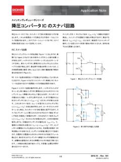
9 , Ltd. All rights reserved. TSZ22111 15 001 Measurement Circuits Figure 12 BA3121F BA3121F 7/12 TSZ02201-0C2C0EZ00390-1-2 2015 ROHM Co., Ltd. All rights reserved. TSZ22111 15 001 Application Information 1. Circuit Operation Figure 13. Flow of Noise in Car Audio Systems Car audio systems are grounded to the car body. For this reason, electrical noise generated by the car electrical system can enter the power Amplifier input through the chassis and become audible. BA3121F utilizes the common-mode rejection characteristics of an operational Amplifier to eliminate this noise.
10 Without BA3121F noise enters the power Amplifier inputs directly. With BA3121F, the CMRR of operational amplifiers 1-A and 2-A eliminates the noise. Principle of noise elimination: To obtain the output voltage (eO) Figure 14. The Principle of Noise Rejection With BA3121F, the elimination level of the noise is expressed as: CMRR = 20log (eO/eI)(eI = e1 = e2) Therefore, CMRR 41dB can be guaranteed. From and 2431324121122434121112)( - - -)( - eRRRRRRReeRReRRRRRReRReO Ideally, if R1R4 = R2R3, and e1 = e2, the noise voltage will be zero.