Transcription of Lead (Pb)-Bearing Thick Film, Rectangular Chip …
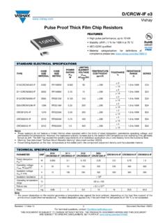
1 Technical questions, contact: Number: 20008118 Revision: 18-Nov-10D/CRCWV ishayLead (Pb)- bearing Thick film , Rectangular chip ResistorsFEATURES Stability R/R = 1 % for 1000 h at 70 C Lead (Pb)- bearing termination plating on Ni barrier layer Metal glaze on high quality ceramic Halogen-free according to IEC 61249-2-21 definiton AEC-Q200 qualified, rev. C compliantNotes These resistors do not feature a limited lifetime when operated within the permissible limits. However, resistance value drift increasing overoperating time may result in exceeding a limit acceptable to the specific application, thereby establishing a functional lifetime. Marking: See datasheet Surface Mount Resistor Marking (document number 20020). Power rating depends on the max. temperature at the solder point, the component placement density and the substrate ELECTRICAL SPECIFICATIONSMODELSIZERATED DISSIPATION P70 WLIMITINGELEMENTVOLTAGEUmax.
2 AC/DCTEMPERATURECOEFFICIENTppm/KTOLERANC E%RESISTANCERANGE SERIESINCH METRICD10/CRCW04020402 RR 100 200 1 51R0 to 10ME24; E96E24 Zero-Ohm-Resistor: Rmax. = 20 m , Imax. = AD11/CRCW0603 0603 RR 100 200 1 51R0 to 10ME24; E96E24 Zero-Ohm-Resistor: Rmax. = 20 m , Imax. = AD12/CRCW08050805 RR 100 200 1 51R0 to 10ME24; E96E24 Zero-Ohm-Resistor: Rmax. = 20 m , Imax. = AD25/CRCW12061206 RR 100 200 1 51R0 to 10ME24; E96E24 Zero-Ohm-Resistor: Rmax. = 20 m , Imax. = ACRCW12101210 RR 100 200 1 51R0 to 10ME24; E96E24 Zero-Ohm-Resistor: Rmax. = 20 m , Imax. = ACRCW12181218 RR 100 200 1 51R0 to 2M2E24; E96E24 Zero-Ohm-Resistor: Rmax. = 20 m , Imax. = ACRCW20102010 RR 100 200 1 51R0 to 10ME24; E96E24 Zero-Ohm-Resistor: Rmax. = 20 m , Imax. = ACRCW25122512 RR 100 200 1 51R0 to 10ME24; E96E24 Zero-Ohm-Resistor: Rmax.
3 = 20 m , Imax. = A Document Number: 20008 For technical questions, contact: 18-Nov-10119D/CRCWLead (Pb)- bearing Thick film , Rectangular chip ResistorsVishayNote(1) The power dissipation on the resistor generates a temperature rise against the local ambient, depending on the heat flow support of theprinted-circuit board (thermal resistance). The rated dissipation applies only if the permitted film temperature of 155 C is not (2)Preferred way for ordering products is by use of the PART SPECIFICATIONSPARAMETERUNITD10/CRCW0402D 11/CRCW0603D12/CRCW0805D25/CRCW1206 CRCW1210 CRCW1218 CRCW2010 CRCW2512 Rated dissipation at 70 C (1) element voltageUMAX. AC/DCV5075150200200200400500 Insulation voltage UINS.(1 min)V> 75> 100> 200> 300> 300> 300> 300> 300 Insulation resistance > 109 Category temperature range C- 55 to + 155 Failure rateh-1< x NUMBER AND PRODUCT DESCRIPTIONPart Number: CRCW0805562 RFKTA (2)MODELVALUETOLERANCETCRPACKAGINGSPECIA LCRCW0402 CRCW0603 CRCW0805 CRCW1206 CRCW1210 CRCW1218 CRCW2010 CRCW2512R = DecimalK = ThousandM = Million0000 = JumperF = 1 %J = 5 %Z = JumperK = 100 ppm/KN = 200 ppm/KS = Jumper or specialTA TBTC TDTE TFTGTHTKUp to 2 digitsProduct Description: CRCW0805 100 562R 1 % RT1 CRCW0805100562R1 %RT1 MODELTCRRESISTANCE VALUETOLERANCEPA C K A G I N GCRCW0402 CRCW0603 CRCW0805 CRCW1206 CRCW1210 CRCW1218 CRCW2010 CRCW2512 100 ppm/K 200 ppm/K10R = 10 562R = 562 10K = k 1M = 1 M 0R0 = Jumper 1 % 5 %RT1 RT5 RT6RT7RF4R02 technical questions, contact: Number: 20008120 Revision.
4 18-Nov-10D/CRCWV ishayLead (Pb)- bearing Thick film , Rectangular chip ResistorsDIMENSIONSPACKAGINGMODELUNITPAP ER TAPEACC. IEC 60286-3, TYPE IBLISTER TAPEACC. IEC 60286-3, TYPE II QUANTITY PART NUMBER PRODUCT DESC. QUANTITY PART NUMBER PRODUCT mm/7"10 000 TDRT7330 mm/13"50 000 TERF4D11/CRCW0603180 mm/7"5000 TART1285 "10 000 TBRT5330 mm/13"20 000 TCRT6D12/CRCW0805180 mm/7"5000 TART1285 "10 000 TBRT5330 mm/13"20 000 TCRT6D25/CRCW1206180 mm/7"5000 TART1285 "10 000 TBRT5330 mm/13"20 000 TCRT6 CRCW1210180 mm/7"5000 TART1285 "10 000 TBRT5330 mm/13"20 000 TCRT6 CRCW1218180 mm/7"4000 TKRT9 CRCW2010180 mm/7"4000 TFR02 CRCW2512180 mm/7"2000 TGR674000 THR82 SIZEDIMENSIONS in millimetersSOLDER PAD DIMENSIONS in millimetersREFLOW SOLDERINGWAVE SOLDERINGINCHMETRICLWHT1T2ab l ab + + + + + Document Number: 20008 For technical questions, contact.
5 18-Nov-10121D/CRCWLead (Pb)- bearing Thick film , Rectangular chip ResistorsVishayFUNCTIONAL PulsePulse Load max. (W)P2512121820101210120608050603040210-6 Pulse Duration i (s)t10-510-410-310-210-1110100 Maximum pulse load, single pulse; applicable if P 0 and n < 1000 and max.;for permissible resistance change equivalent to 8000 h Continuous PulseMaximum pulse load, continuous pulses; applicable if P P ( amb) and max.;for permissible resistance change equivalent to 8000 h operationPulse Duration i (s)Continuous Pulse Load max. (W)tP10010-510-410-310-210-1110100251212 182010121012060805060304022000200010- 610- 510- 410- 310- 210- 1 110 Pulse VoltageMaximum pulse voltage, single and continuous pulses; applicable ifP Pmax.; for permissible resistance change equivalent to 8000 h operationPulse Duration i (s)40060080010001200140016001800 Pulse Voltage max.
6 (V)251220101206/1210/1218080506030402t technical questions, contact: Number: 20008122 Revision: 18-Nov-10D/CRCWV ishayLead (Pb)- bearing Thick film , Rectangular chip Resistors- 55- 250255075100125155 17512010080604020070 DeratingAmbient Temperature in CFraction of Rated Dissipation in %10120 Resistance Value R in Attenuation of 3rd Harmonic A3 in dBNon-Linearity1008040602001001K10K100K1 M10M1206, 20100805060304021001K10K100K1M10M100 10 Noise A1 in V/VCurrent Noise20101206080506030402 Resistance Value R in Document Number: 20008 For technical questions, contact: 18-Nov-10123D/CRCWLead (Pb)- bearing Thick film , Rectangular chip ResistorsVishayTEST PROCEDURES AND REQUIREMENTSEN 60115-1 CLAUSEIEC 60082-2 TEST METHODTESTPROCEDUREREQUIREMENTS PERMISSIBLE CHANGE ( R)STABILITY CLASS 1 OR BETTERSTABILITY CLASS 2 OR BETTERS tability for product types:1 to 10 M 1 to 10 M 1 % 5 % proofU = Uins; 60 sNo flashover or breakdown time overloadU= x 2 x Umax.
7 ;duration: Acc. to style ( % R + ) ( % R + ) (Td)SolderabilitySolder bath method; Sn60Pb40;non-activated flux; (235 5) C, (2 ) sGood tinning ( 95 % covered);no visible coefficient(20/- 55/20) C and(20/125/20) C 100 ppm/K 200 (Uu3)Shear (adhesion)RR 1608 and smaller: 9 NRR 2012 and larger: 45 NNo visible (Uu1)Substrate bendingDepth 2 mm; 3 timesNo visible damage, no open circuit in bent position ( % R + ) (Na)Rapid change of temperature30 min. at - 55 C;30 min. at 125 C5 cycles1000 cycles ( % R + ) (1 % R + ) ( % R + ) (1 % R + ) sequence:- (1 % R + ) (2 % R + ) (Ba)Dry heat125 C; 16 h (Db)Damp heat, cyclic55 C; 90 % RH; 24 h; 1 (Aa)Cold- 55 C; 2 (M)Low air pressure1 kPa; (25 10) C; 1 (Db)Damp heat, cyclic55 C; 90 % RH; 24 h; 5 loadU= at 70 CU = (P70 x R) h on; h off;70 C; 1000 h70 C; 8000 h (1 % R + ) (2 % R + ) (2 % R + ) (4 % R + ) (Td)Resistance to soldering heatSolder bath method(260 5) C; (10 1) s ( % R + ) ( % R + ) , needle flame testIEC 60695-11-5; 10 sNo burning after 30 (Cab)Damp heat, steady state(40 2) C;(93 3) % RH; 56 days (1 % R + ) at uppercategory temperature155 C; 1000 h (1 % R + ) (2 % R + ) discharge(human body model) IEC 61340-3-1;3 pos.
8 + 3 neg. discharges; ESD test voltage acc. to size (1 % R + ) (XA)Component solvent resistanceIsopropyl alcohol; 50 C; method 2No visible (XA)Solvent resistance of markingIsopropyl alcohol; 50 C; method 1, toothbrushMarking legible, no visible damageP70 x RP70 x technical questions, contact: Number: 20008124 Revision: 18-Nov-10D/CRCWV ishayLead (Pb)- bearing Thick film , Rectangular chip ResistorsAll tests are carried out in accordance with the following specifications: EN 60115-1, generic specification EN 140400, sectional specification EN 140401-802, detail specification IEC 60068-2, environmental test proceduresPackaging of components is done in paper or blister tapes according to IEC (Fc)Vibration, endurance bysweepingf = 10 Hz to 2000 Hz; x, y, z mm; A 200 m/s2;10 sweeps per axis ( % R + ) ( % R + ) electric overloadU= 2 x Umax.
9 ; s on; s off;1000 cycles (1 % R + ) pulse high voltage overload, 10 s/700 s = 10 x 2 x Umax.;10 pulses (1 % R + 0,05 )TEST PROCEDURES AND REQUIREMENTSEN 60115-1 CLAUSEIEC 60082-2 TEST METHODTESTPROCEDUREREQUIREMENTS PERMISSIBLE CHANGE ( R)STABILITY CLASS 1 OR BETTERSTABILITY CLASS 2 OR BETTERS tability for product types:1 to 10 M 1 to 10 M D/CRCW15 x P70 x RP70 x R Legal Disclaimer Revision: 08-Feb-171 Document Number: 91000 Disclaimer ALL PRODUCT, PRODUCT SPECIFICATIONS AND DATA ARE SUBJECT TO CHANGE WITHOUT NOTICE TO IMPROVE RELIABILITY, FUNCTION OR DESIGN OR OTHERWISE. vishay Intertechnology, Inc., its affiliates, agents, and employees, and all persons acting on its or their behalf (collectively, vishay ), disclaim any and all liability for any errors, inaccuracies or incompleteness contained in any datasheet or in any other disclosure relating to any makes no warranty, representation or guarantee regarding the suitability of the products for any particular purpose or the continuing production of any product.
10 To the maximum extent permitted by applicable law, vishay disclaims (i) any and all liability arising out of the application or use of any product, (ii) any and all liability, including without limitation special, consequential or incidental damages, and (iii) any and all implied warranties, including warranties of fitness for particular purpose, non-infringement and merchantability. Statements regarding the suitability of products for certain types of applications are based on vishay s knowledge of typical requirements that are often placed on vishay products in generic applications. Such statements are not binding statements about the suitability of products for a particular application. It is the customer s responsibility to validate that a particular product with the properties described in the product specification is suitable for use in a particular application.