Transcription of Pulse Proof Thick Film Chip Resistors - Vishay
1 D/CRCW-IF Revision: 17-Mar-151 Document Number: 20024 For technical questions, contact: DOCUMENT IS SUBJECT TO CHANGE WITHOUT NOTICE. THE PRODUCTS DESCRIBED HEREIN AND THIS DOCUMENTARE SUBJECT TO SPECIFIC DISCLAIMERS, SET FORTH AT Proof Thick Film Chip ResistorsFEATURES High Pulse performance, up to 10 kW Stability R/R 1 % for 1000 h at 70 C AEC-Q200 qualified Material categorization: for definitions of compliance please see Notes These Resistors do not feature a limited lifetime when operated within the limits of rated dissipation, permissible operating voltage, and permissible film temperature. However, the resistance typically increase due to the resistor s film temperature over operating time, generally known as drift.
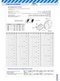
2 The drift may exceed the stability requirements of an individual application circuit and thereby limits the functional time. Marking: See data sheet Surface Mount Resistor Marking (document number 20020). Power rating depends on the max. temperature at the solder point, the component placement density and the substrate (1)The power dissipation on the resistor generates a temperature rise against the local ambient, depending on the heat flow support of the printe-circuit board (thermal resistance). The rated dissipation applies only if the permitted film temperature of 155 C is not ELECTRICAL SERIESD10 200 to 100KE24 10D11 200 to 100KE24 10D12 200 to 100KE24 10D25 200 to 100KE24 200 to 100KE24 200 to 100KE24 200 to 100KE24 10 TECHNICAL SPECIFICATIONSPARAMETERUNITD10/CRCW0402- IFD11/CRCW0603-IFD12/CRCW0805-IFD25/CRCW 1206-IFCRCW1210-IF CRCW2010-IF CRCW2512-IFRated dissipation P70 (1) voltage Umax.
3 ACRMS/DCV5075150200200400500 Insulation voltage Uins (1 min)V75100200300300300300 Insulation resistance > 109 Operating temperature range C-55 to +155 Failure rateh-1< x Revision: 17-Mar-152 Document Number: 20024 For technical questions, contact: DOCUMENT IS SUBJECT TO CHANGE WITHOUT NOTICE. THE PRODUCTS DESCRIBED HEREIN AND THIS DOCUMENTARE SUBJECT TO SPECIFIC DISCLAIMERS, SET FORTH AT NUMBER AND PRODUCT DESCRIPTIONPart Number: CRCW08051R00 JNEAIFTYPEVALUETOLERANCETCRPACKAGINGSPEC IALCRCW0402 CRCW0603 CRCW0805 CRCW1206 CRCW1210 CRCW2010 CRCW2512R = DecimalK = ThousandJ = 5 %K = 10 %N = 200 ppm/KEA, EB,EC, ED,EE, EF,EG, EH,EI, ELUp to 2 digitsIF = Pulse proofProduct Description: D12/CRCW0805-IF 200 1R0 5 % ET1 e3D12/CRCW0805-IF2001R05 %ET1e3 TYPETCRRESISTANCE VALUETOLERANCEPACKAGINGLEAD (Pb)-FREED10/CRCW0402-IFD11/CRCW0603-IFD 12/CRCW0805-IFD25/CRCW1206-IFCRCW1210-IF CRCW2010-IFCRCW2512-IF 200 ppm/K1R0 = 1 10K = 10 k 5 % 10 %ET1, ET2,ET3, ET4,ET5, ET6,ET7, ET8,ET9, EF4,E02, E67,E82e3 = Pure tin termination finishPACKAGINGTYPECODEQUANTITYCARRIER TAPEWIDTHPITCHREEL DIAMETERD10/CRCW0402-IFED = ET710 000 Paper tape acc.
4 ToIEC 60286-3 Type 1a8 mm 2 mm 180 mm/7"EE = EF450 000330 mm/13"D11/CRCW0603-IFEI = ET250008 mm2 mm 180 mm/7"ED = ET310 000180 mm/7"EL = ET420 000285 "EE = ET850 000330 mm/13"EA = ET150008 mm4 mm180 mm/7"EB = ET510 000285 "EC = ET620 000330 mm/13"D12/CRCW0805-IFEA = ET150008 mm4 mm180 mm/7"EB = ET510 000285 "EC = ET620 000330 mm/13"D25/CRCW1206-IFEA = ET150008 mm4 mm180 mm/7"EB = ET510 000285 "EC = ET620 000330 mm/13"CRCW1210-IFEA = ET150008 mm4 mm180 mm/7"EB = ET510 000285 "EC = ET620 000330 mm/13"CRCW2010-IFEF = E024000 Pressed tapeacc. toIEC 60286-3 Type 1b12 mm4 mm180 mm/7"CRCW2512-IFEG = E67200012 mm 8 mm 180 mm/7"EH = E8240004 mmCW08051R00 NAFCRJE ID/CRCW-IF Revision: 17-Mar-153 Document Number: 20024 For technical questions, contact: DOCUMENT IS SUBJECT TO CHANGE WITHOUT NOTICE.
5 THE PRODUCTS DESCRIBED HEREIN AND THIS DOCUMENTARE SUBJECT TO SPECIFIC DISCLAIMERS, SET FORTH AT PERFORMANCEDIMENSIONS in millimetersSIZEDIMENSIONSRECOMMENDED SOLDER PAD DIMENSIONSREFLOW SOLDERINGWAVESOLDERINGIMPERIAL + - + - + - + - Pulse load, single Pulse ; applicable if P 0 and n 1000 and max.;for permissible resistance change equivalent to 8000 h operationPulse Duration (s) Pulse Power (W) 000251220101210120608050603040210 000 Maximum Pulse dissipation as a function of the Pulse duration,single pulseD/CRCW-IF Revision: 17-Mar-154 Document Number: 20024 For technical questions, contact: DOCUMENT IS SUBJECT TO CHANGE WITHOUT NOTICE.
6 THE PRODUCTS DESCRIBED HEREIN AND THIS DOCUMENTARE SUBJECT TO SPECIFIC DISCLAIMERS, SET FORTH AT Pulse load, continuous pulses; applicable if P P ( amb) and max.;for permissible resistance change equivalent to 8000 h operationPulse Duration (s) Pulse Power (W) 000251220101210120608050603040210 000 Maximum Pulse dissipation as a function of the Pulse duration,continuous Pulse loading2000200010- 610- 510- 410- 310- 210- 1 110 Maximum Pulse voltage, single and continuous pulses; applicable ifP Pmax.; for permissible resistance change equivalent to 8000 h operationPulse Duration i (s)40060080010001200140016001800 Pulse Voltage max. (V)25121206/1210080506030402t 2010D/CRCW-IF Revision: 17-Mar-155 Document Number: 20024 For technical questions, contact: DOCUMENT IS SUBJECT TO CHANGE WITHOUT NOTICE.
7 THE PRODUCTS DESCRIBED HEREIN AND THIS DOCUMENTARE SUBJECT TO SPECIFIC DISCLAIMERS, SET FORTH AT 000100 00011010 00010010002512201012101206080506030402 Resistance Value ( )Peak Voltage (V) Pulse load rating in accordance to EN 60115-1, ; s/50 s;5 pulses at 12 s intervals; for permissible resistance change 1 %Single- Pulse high voltage overload test s/50 s EN 140000 000100 000 Resistance Value ( )Peak Voltage (V)11010 0001001000 Pulse load rating in accordance to EN 60115-1, ; 10 s/700 s;10 pulses at 1 min intervals; for permissible resistance change 1 %Single- Pulse high voltage overload test 10 s/700 s EN 140000 Revision: 17-Mar-156 Document Number: 20024 For technical questions, contact: DOCUMENT IS SUBJECT TO CHANGE WITHOUT NOTICE.
8 THE PRODUCTS DESCRIBED HEREIN AND THIS DOCUMENTARE SUBJECT TO SPECIFIC DISCLAIMERS, SET FORTH AT PROCEDURES AND REQUIREMENTSEN 60115-1 CLAUSEIEC 60082-2 TEST METHODTESTPROCEDUREREQUIREMENTS PERMISSIBLE CHANGE ( R)STABILITY CLASS 1 OR BETTERS tability for product type:1 to 100 k D/CRCW-IF 5 %; 10 % proofU = x Uins; 60 sNo flashover or breakdown time overloadU = x 2 x Umax.;duration acc. to style ( % R + ) (Td)SolderabilitySolder bath method; Sn60Pb40;non-activated flux; (235 5) C, (2 ) sGood tinning ( 95 % covered);no visible damageSolder bath method; ;non-activated flux; (245 5) C, (3 ) sGood tinning ( 95 % covered);no visible coefficient(20/- 55/20) C and(20/125/20) C 200 (Na)Rapid change of temperature30 min.
9 At - 55 C;30 min. at 125 C5 cycles1000 cycles ( % R + ) (1 % R + )- 50050100150 Ambient Temperature amb ( C)Fraction of Rated Dissipation P70 (%)050100 Derating70P70 x RD/CRCW-IF Revision: 17-Mar-157 Document Number: 20024 For technical questions, contact: DOCUMENT IS SUBJECT TO CHANGE WITHOUT NOTICE. THE PRODUCTS DESCRIBED HEREIN AND THIS DOCUMENTARE SUBJECT TO SPECIFIC DISCLAIMERS, SET FORTH AT tests are carried out in accordance with the following specifications: EN 60115-1, generic specification EN 140400, sectional specification EN 140401-802, detail specification IEC 60068-2-x, environmental test proceduresPackaging of components is done in paper or blister tapes according to IEC sequence:- (1 % R + ) (Ba)Dry heat125 C; 16 h (Db)Damp heat, cyclic55 C; 90 % RH; 24 h; 1 (Aa)Cold- 55 C; 2 (M)Low air pressure1 kPa; (25 10) C; 1 (Db)Damp heat, cyclic55 C; 90 % RH; 24 h; 5 loadU = at 70 CU = h on; h off;70 C; 1000 h70 C.
10 8000 h (1 % R + ) (2 % R + ) (Td)Resistance to soldering heatSolder bath method(260 5) C; (10 1) s ( % R + ) (Cab)Damp heat, steady state(40 2) C;(93 3) % RH; 56 days (1 % R + ) at uppercategory temperature155 C; 1000 h (1 % R + ) Pulse high voltage overload, 10 s/700 s = 10 x 2 x Umax.;10 pulses (1 % R + )TEST PROCEDURES AND REQUIREMENTSEN 60115-1 CLAUSEIEC 60082-2 TEST METHODTESTPROCEDUREREQUIREMENTS PERMISSIBLE CHANGE ( R)STABILITY CLASS 1 OR BETTERS tability for product type:1 to 100 k D/CRCW-IF e3P70 x RP70 x RP70 x RLegal Disclaimer Revision: 01-Jan-20191 Document Number: 91000 Disclaimer ALL PRODUCT, PRODUCT SPECIFICATIONS AND DATA ARE SUBJECT TO CHANGE WITHOUT NOTICE TO IMPROVE RELIABILITY, FUNCTION OR DESIGN OR OTHERWISE.