Transcription of Low-Voltage MIL-COTS Input Filter Module
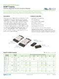
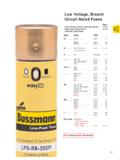
1 LV MFM FilterLow- voltage MIL-COTS Input Filter ModuleMFM1714x50M50C5yzzLV MFM Filter Rev 1 of 16 07/2018 Features & Benefits 28V nominal Input 99% efficiency EMI filtering MIL-STD-461E/F, selected CE and CS tests Input transient protection MIL-STD-1275A/B/D/E MIL-STD-704A/F (MIL-HDBK-704-8)Normal and abnormal transients Envronmental qualification MIL-STD-810 MIL-STD-202 Low M-Grade temperature rating,providing operation down to 55 C Output power up to 350W Available in chassis and PCB mount Small size x x [ x x ]Typical Applications Defense AerospaceCompatible Products Low Input voltage DCM3414 VIA Low Input voltage ChiP [a] DCMP roduct DescriptionThe MFM DCM Filter is a DC front-end Module that provides EMI filtering and transient protection. The MFM DCM Filter enables designers using Vicor 28V nominal Input voltage VIA or ChiP [a] modules to meet conducted emission/conducted susceptibility per MIL-STD-461E/F; and Input transients per MIL-STD-704A/F, MIL-STD-1275A/B/D/E and DO-160E.
2 The MFM DCM Filter accepts an Input voltage of 16 50 VDC (28V nominal Input ) and delivers output power up to x x [ x x ]Part Ordering InformationProductFunctionPackage LengthPackageWidthPackageTypeMaxHighSide VoltageHigh Side VoltageRangeRatioMax LowSide VoltageMaxLowSide CurrentProductGrade(Case Temperature)Option FieldMFM1714x50M50C5yzzMFM = MIL-COTS Input Filter ModuleLength in Inches x 10 Width in Inches x 10B = Board VIAV = Chassis VIAI nternal ReferenceM = 55 to 100 C00 = Chassis04 = Short Pin08 = Long Pin[a]Additional components are required for EMI filtering and transientsuppression, when used with ChiP package MFM Filter Rev 2 of 16 07/2018 MFM1714x50M50C5yzz16 50 VSource VDDEEN TR SENSE +SENSE LOADMFM+IN +OUTEMI GND IN+IN IN OUT+OUT OUTearth ground DCM3414 VIA CINCIN-DCMCOUT-EXTFM-Grade DCM3414 VIA with an MFM Input Filter , to meet the EMI and transient requirementsTypical ApplicationParts List for Typical ApplicationsFEATON (Cooper/Bussman)
3 ABC series, fast-acting tube fuses rated 30 ALittlefuse NANO2 456 Series, surface-mount fuses rated 30 ALV MFM Filter Rev 3 of 16 07/2018 MFM1714x50M50C5yzzMFM1714 Filter Chassis (Lug) Mount Terminals UpMFM1714 Filter PCB Mount Pins Down+IN IN+OUT OUTEMIGND IN+IN OUT+OUTEMIGNDPin ConfigurationPin DescriptionsSignal NameTypeFunction+ININPUT POWERP ositive Input power terminal ININPUT POWER RETURNN egative Input power terminalEMI GNDEMI GROUNDEMI ground terminal+OUTOUTPUT POWERP ositive output power terminal OUTOUTPUT POWER RETURNN egative output power terminalNote: These pin drawings are not to MFM Filter Rev 4 of 16 07/2018 MFM1714x50M50C5yzzAbsolute Maximum RatingsThe absolute maximum ratings below are stress ratings only. Operation at or beyond these maximum ratings can cause permanent damage to the device.
4 Electrical specifications do not apply when operating beyond rated operating voltage (+IN to IN)Continuous per MIL-STD-1275D/E, 50ms100 Transient per MIL-STD-1275A/B/D, 70 s250 Transient per DO-160E, 100ms80 Output voltage (+OUT to OUT)Continuous Withstand ( Input /Output to EMI GND/Case)1500 VDCS torage TemperatureM-Grade 65125 CInternal Operating TemperatureM-Grade 55125 CAverage Output Current22 AInput/Output Pin Torque and Mounting Torque4 ( ) ( )Electrical SpecificationsSpecifications apply over all line and load conditions, unless otherwise noted; boldface specifications apply over the temperature range of 55 C TCASE 100 C (M-Grade); all other specifications are at TCASE = 25 C unless otherwise / NotesMinTypMaxUnitPower Input / Output SpecificationInput voltage Range [b]VINC ontinuous operation162850 VTransient per MIL-STD-1275D/E, 50ms100 Transient per MIL-STD-1275A/B/D, 70 s250 Transient per DO-160E, 100ms80 Maximum Output Current [c]IOUT_MAXC ontinuous, at VOUT = 16V (IOUT = POUT/VIN)22 ARated Output Power [c]POUTC ontinuous, over all line conditions350 WInternal voltage Drop@16V, 22A, 100 C Full load, low line, high load, nominal line, high temperature load, high line, high [b] Transient immunity specifications are met only when LV MFM is used with M-Grade 16 50 VIN DCM3414 VIA.
5 [c] One MFM for each DCM even if the total power of the DCM is below POUT maximum MFM Filter Rev 5 of 16 07/2018 MFM1714x50M50C5yzzEMI/EMCS tandardTest ProcedureNotesMIL-STD-461E/FConducted EmmisionsCE101 Figure CE101-4, Navy ASW & Army Aircraft, Curve #2 (28 VDC or below)CE102 Figure CE102-1, Basic curve for all applicationsConducted SusceptibilityCS101 Figure CS101, Curve #2, for all applications (28 VDC or below)MIL-STD-1275 Transient Immunity [d]MIL-STD-1275A/B/D/E100 VDC for 50ms duration250 VDC for 70 sMIL-STD-704 Transient Immunity [d]MIL-STD-704A (MIL-HDBK-704-8) Normal voltage TransientsFrom table LDC 105-II (A-J) overvoltage 70 VDC for 20ms duration; within the MIL-STD-1275 (100V for 50ms) transient conditionMIL-STD-704B/C/D/E/F (MIL-HDBK-704-8) Normal voltage TransientsFrom table LDC 105-III (AA-RR) overvoltage 50 VDC for duration, undervoltage 18 VDC for 15ms duration; within the normal operating Input voltage rangeMIL-STD-704A (MIL-HDBK-704-8) Abnormal voltage TransientsFrom table LDC 302-II (A-J) overvoltage 80 VDC for 50ms duration; within the MIL-STD-1275 (100V for 50ms) transient conditionMIL-STD-704E/F (MIL-HDBK-704-8) Abnormal voltage TransientsFrom Table LDC 302-IV (AAA-FFF), overvoltage test conditions; within the normal operating Input voltage rangeDO-160 ETransient Immunity [d]DO-160E sec.
6 16, cat. z80 VDC for 100ms[d] Transient immunity specifications are met only when LV MFM is used with M-grade 16 50 VIN DCM3414 VIA .LV MFM Filter Rev 6 of 16 07/2018 MFM1714x50M50C5yzzTypical CharacteristicsFrequency (Hz)Common Mode-60-70-80-901k10010k100k1M10M-50-40- 30-20-100 Differential ModeAttenuation (dB) F/Hz CM-Mode DF-ModeCursor 1 100k 2 1M Impedance Mangitude Z (dB ): Output Impedance Mangitude Z ( )Frequency (Hz)Output Impedance Z (dB )Output Impedance Z ( )Figure 1 Attenuation (dB) vs. frequency (Hz), Input leads are terminated with LISN impedances 25 for common mode, 100 for differential modeFigure 2 Output impedance vs. frequency (Hz) plot looking back into the output terminals of the MFM with shorted Input terminalsLV MFM Filter Rev 7 of 16 07/2018 MFM1714x50M50C5yzzTypical Conducted EmissionsCE101 peak scans with MFM1714V50M50C5M00 and DCM3414V50M31C2T01, in either condition: OUT connected to GND or OUT Hz10 kHzSGL1 MAUnitdBA 2016 14:25 ResBW 100 HzMeas T 20 msDetMAAtt 10 dBINPUT 2100 Hz1 kHz10 kHz 10 20 30 40 50 60 70 80 90 100 110 120 130 0 140CE101-42 Date: 14:25:3930 Hz10 kHzSGL1 MAUnitdBA TrdCE101 ResBW 100 HzMeas T 20 msDetMAAtt 10 dBINPUT 2016 14:06100 Hz1 kHz10 kHz 10 20 30 40 50 60 70 80 90 100 110 120 130 0 1401 Marker 1 [T1] dBA Hz 1 [T1] dBA Hz CE101-42 Date: 14:06:2730 Hz10 kHzSGL1 MAUnitdBA 2016 14.
7 40 DetMAResBW 10 HzMeas T 20 msAtt 10 dBINPUT 2100 Hz1 kHz10 kHz 10 20 30 40 50 60 70 80 90 100 110 120 130 0 1401 Marker 1 [T1] dBA Hz 1 [T1] dBA Hz CE101-42 Date: 14:40:36 Figure 4 Peak scan for the RED lead with CIN = 2200 F, COUT-EXT = 1000 F, 0% loadFigure 7 Peak scan for the BLACK lead with CIN = 2200 F, COUT-EXT = 1000 F, 100% loadFigure 5 Peak scan for the RED lead with CIN = 2200 F, COUT-EXT = 1000 F, 100% load30 Hz10 kHzSGL1 MAUnitdBA TrdCE101 ResBW 100 HzMeas T 20 msDetMAAtt 10 dBINPUT 2016 14:21100 Hz1 kHz10 kHz 10 20 30 40 50 60 70 80 90 100 110 120 130 0 140CE101-42 Date: 14:21:38 Figure 6 Peak scan for the BLACK lead with CIN = 2200 F, COUT-EXT = 1000 F, 0% loadDC Power SupplyScreenRoom/FiltersLISNLISNLV MFM+IN+OUT OUT IN+IN+OUTLoad50 Termination onSignal Output Port(One for Each LISN)EMIR eceiverCurrent ProbeEMI GND+ CINCOUTDCM3414 VIA OUT INFigure 3 A typical test set up for conducted emissions CE101 is shown above.
8 A current probe is used to measure and plot the variations in the current through the RED and BLACK leads at various load MFM Filter Rev 8 of 16 07/2018 MFM1714x50M50C5yzzTypical Conducted Emissions (Cont.)CE102 peak scans with MFM1714V50M50C5M00 and DCM3414V50M31C2T01, in either condition: OUT connected to GND or OUT kHz10 MHzUnitdBV 2016 15:24 ResBW 10 kHzMeas T 20 msDetMAAtt 10 dBINPUT 2100 kHz1 MHz10 MHz 20 30 40 50 60 70 80 90 100 10 1101 Marker 1 [T1] dBV kHz1 [T1] dBV kHzCE10228 Date: 15:24:45 SGL1MA10 kHz10 MHzUnitdBV 2016 15:32 ResBW 10 kHzMeas T 20 msDetMAAtt 10 dBINPUT 2100 kHz1 MHz10 MHz 20 30 40 50 60 70 80 90 100 10 1101 Marker 1 [T1] dBV kHz1 [T1] dBV kHzCE10228 Date: 15:32:50 SGL1MA10 kHz10 MHzUnitdBV TrdCE102 REDResBW 10 kHzMeas T 20 msDetMAAtt 10 dBINPUT 2016 15.
9 19100 kHz1 MHz10 MHz 20 30 40 50 60 70 80 90 100 10 1101 Marker 1 [T1] dBV kHz1 [T1] dBV kHzCE10228 Date: 15:19:13 Figure 9 Peak scan for the RED lead with CIN = 2200 F, CIN-DCM = 1000 F, COUT-EXT = 1000 F, 0% loadFigure 12 Peak scan for the BLACK lead with CIN = 2200 F, CIN-DCM = 1000 F, COUT-EXT = 1000 F, 100% loadFigure 10 Peak scan for the RED lead with CIN = 2200 F, CIN-DCM = 1000 F, COUT-EXT = 1000 F, 100% loadSGL1MA10 kHz10 MHzUnitdBV 2016 15:26 ResBW 10 kHzMeas T 20 msDetMAAtt 10 dBINPUT 2100 kHz1 MHz10 MHz 20 30 40 50 60 70 80 90 100 10 1101 Marker 1 [T1] dBV kHz1 [T1] dBV kHzCE10228 Date: 15:26:59 Figure 11 Peak scan for the BLACK lead with CIN = 2200 F, CIN-DCM = 1000 F, COUT-EXT = 1000 F, 0% loadDC Power SupplyScreenRoom/FiltersLISNLISN50 Termination+ EMI Reciever20dB AttenuatorLV MFM IN+IN+OUT OUTLoadEMI GNDDCM3414 VIA CIN-DCMCINCOUT IN+IN+OUT OUTF igure 8 A typical test set up for conducted emissions CE102 is shown above.
10 A 50 termination is used for LISN and voltage across the RED and BLACK leads are measured at various load MFM Filter Rev 9 of 16 07/2018 MFM1714x50M50C5yzzElectrical Power CharacteristicsTransient immunity with MFM1714V50M50C5M00 and DCM3414V50M13C2M01 per MIL-STD-1275 14 Transient immunity; LV MFM and DCM3414 VIA output response to an 100V, 50ms Input transientCH1CH2CH4CH32nd Stage EMI Filter & Transient Suppression16 50 VSource LOADLV MFM+IN +OUTEMI GND IN+IN IN+IN_ChiP DCMVIN_ChiP DCM IN_ChiP DCM OUT+OUT OUTearth groundNote: Input line transients are clamped to maximum acceptable Input voltage (VIN_ChiP DCM) using two stages of active transient suppression : A 100V, 50ms Input line transient is clamped as follows:1. LV MFM clamps 100V to DCM3414 VIA Input transient circuit clamps 80V to VIN_ChiP DCM = VIN.
