Transcription of Microwave Amplifiers
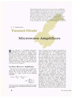
1 EEE 194 RF - 1 - 1994-99 D. B. Leeson Microwave Amplifiers Design of Microwave Transistor Amplifiers Using S Parameters Microwave Amplifiers combine active elements with passive transmission line circuits to provide functions critical to Microwave systems and instruments. The history of Microwave Amplifiers begins with electron devices using resonant or slow-wave structures to match wave velocity to electron beam velocity. The design techniques used for BJT and FET Amplifiers employ the full range of concepts we have developed in the study of Microwave transmission lines, two-port networks and Smith chart presentation. The development of S-parameter matrix concepts grew from the need to characterize active devices and Amplifiers in a form that recognized the need for matched termination rather than short- or open-circuit termination.
2 Much of the initial work was performed at the Hewlett-Packard Company in connection with the development of instruments to measure device and amplifier parameters. We'll begin by considering Microwave Amplifiers that are 1) Small signal so that superposition applies, and 2) Built with Microwave bipolar junction or field-effect transistors References The following books and notes are references for this material: Pozar1, D. M., Microwave Engineering Gonzalez2, G., Microwave Transistor Amplifiers Vendelin, Pavio & Rohde3, Microwave Circuit Design Using Linear and Nonlinear Techniques Review of Transmission Lines 1 Pozar, D.
3 , Microwave Engineering, 2nd Edition, J. Wiley, 1998, pg. 600-640 2 Gonzalez, G., Microwave Transistor Amplifiers , 3 Vendelin, Pavio & Rohde, Microwave Circuit Design Using Linear and Nonlinear Techniques, J. Wiley, 1990 - 2 - For the purpose of characterizing Microwave Amplifiers , key transmission line concepts are 1) Traveling waves in both directions, V+ and V- 2) Characteristic impedance Zo and propagation constant j 3) Reflection coefficient =ZL - ZoZL + Zo for complex load ZL 4) Standing waves resulting from 0 5) Transformation of ZL through line of Zo and length l 6) Description of and Z on the Smith chart (polar graph of ) Review of Scattering Matrix 1) Normalization with respect to Zo of wave amplitudes: a = V+Zo and b = V-Zo 2) Relationship of bi and ai.
4 Bi = i ai 3) Expressions for b1 and b2 at reference planes: b1 = S11a1 + S12a2 b2 = S21a1 + S22a2 4) Definitions of Sii: S11 = b1a1 for a2 = 0, , input for output terminated in Zo. S21 = b2a1 for a2 = 0, , forward transmission ratio with Zo load. S22 = b2a2 for a1 = 0, , output for input terminated in Zo. S21 = b1a2 for a1 = 0, , reverse transmission ratio with Zo source. lS21l2 = Transducer power gain with Zo source and load. 5) Definitions of L, s, in and out: L = ZL - ZoZL + Zo , the reflection coefficient of the load s = Zs - ZoZs + Zo , the reflection coefficient of the source in = Zin - ZoZin + Zo = S11+S12S21 L1-S22 L , the input reflection coefficient out = Zout - ZoZout + Zo = S22+S12S21 s1-S11 s , the output reflection coefficient 6) Power Gain G, Available Gain GA, Transducer Gain GT.
5 - 3 - G = PLPin = power delivered to the loadpower input to the network GA = PavoutPavs = power available from the networkpower available from the source GT = PLPavs = power delivered to the loadpower available from the source Modeling of Microwave Transistors and Packages The S parameters of a given Microwave transistor can be derived from transistor equivalent circuit models based on device physics, or they can be measured directly. Generally, a manufacturer of a device intended for Microwave applications will provide extensive S-parameter data to permit accurate design of Microwave Amplifiers . This can be verified by measurement, a step that has proven important on many occasions.
6 For a bipolar junction transistor, in addition to intrinsic device parameters such as base resistance and collector-base capacitance, amplifier performance is strongly affected by the so-called parasitic elements associated with the device package, including base-lead and emitter-lead inductance internal to the package. Similar considerations apply to Microwave field-effect transistors. The magnitude and phase angle of each of the S parameters typically vary with frequency, and characterization over the complete range of interest is necessary. An abridged table from Pozar4 typical of S-parameter data (Zo=50 ) is shown here for a Microwave FET: f GHz S11 S21 S12 S22 Power Gain Equations The equations for the various power gain definitions are 4 Pozar, D.
7 , Microwave Engineering, 2nd Edition, J. Wiley, 1998, pg. 620 - 4 - 1) G = PLPin = 11 - l inl2 lS21l2 1 - l Ll2l1 - S22 Ll2 2) GA = PavoutPavs = 1 - l sl2l1 - S11 sl2 lS21l2 11 - l outl2 3) GT = PLPavs = 1 - l sl2l1 - in sl2 lS21l2 1 - l Ll2l1 - S22 Ll2 = 1 - l sl2l1 - S11 sl2 lS21l2 1 - l Ll2l1 - out Ll2 The expressions for in and out are 1) in = S11+S12S21 L1-S22 L 2) out = S22+S12S21 s1-S11 s For a unilateral network, S12=0 and 1) in = S11 if S12=0 (unilateral network) 2) out = S22 if S12=0 (unilateral network) The transducer gain GT can be expressed as the product of three gain contributions GT=GsGoGL, where Go = lS21l2 Gs = 1 - l sl2l1 - in sl2 and GL = 1 - l Ll2l1 - S22 Ll2 - 5 - ZoZo sin out L Input Matching Circuit G sOutput Matching Circuit G LTransistor [S] G o If the device is unilateral, or sufficiently so that S12 is small enough to be ignored, the unilateral transducer gain GTU is simplified because GsU = 1 - l sl2l1 - S11 sl2 , where the subscript U indicates unilateral gain.
8 In practice, the difference between GT and GTU is often quite small, as it is desirable for devices to be unilateral if possible. The components of GTU can also be expressed in decibel form, so that GTU (dB) = Gs (dB) + Go (dB) + GL (dB). We can maximize Gs and GL by setting s = S11* and L = S22* so that Gsmax = 11 - lS11l2 and GLmax = 11 - lS22l2 , so that GTUmax = 11 - lS11l2 lS21l2 11 - lS22l2 Note that, if lS11l=1 or lS22l=1, GTUmax is infinite. This raises the question of stability, which will be examined next. Stability In a two-port network, oscillations are possible if the magnitude of either the input or output reflection coefficient is greater than unity, which is equivalent to presenting a negative resistance at the port.
9 This instability is characterized by - 6 - l inl > 1 or l outl > 1, which for a unilateral device implies lS11l > 1 or lS22l > 1. Thus the requirements for stability are l inl = lS11+S12S21 L1-S22 L l < 1 and l outl = lS22+S12S21 s1-S11 s l < 1 These are defined by circles, called stability circles, that delimit l inl = 1 and l Ll = 1 on the Smith chart. The radius and center of the output and input stability circles are derived from the S parameters on pg. 614 of Pozar or pg. 97 of Gonzalez. The concept of instability with varying input or output matching conditions is significant, as we would desire an amplifier to be unconditionally stable under all expected conditions of source and load impedances.
10 The example of input stability circles is shown here. This same derivation can be accomplished analytically. The conditions for stability are K = 1 - lS11l2 - lS22l2 + l l22 - lS12S21l > 1 and l l < 1, where , the determinant of the scattering matrix, is = S11S22 - S12S21 If an amplifier is conditionally stable, it can be rendered unconditionally stable by adding resistance to the input and/or output of the amplifier so that the total loop resistance at the input and output is positive. The use of resistive loading or feedback can compromise the - 7 - noise performance of an amplifier unless accomplished in connection with an analysis of the amplifier noise figure.