Transcription of MSC8256 Six-Core Digital Signal Processor - Data Sheet
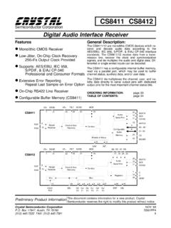
1 FC-PBGA 78329 mm 29 mmFreescale SemiconductorData Sheet 2008 2013 Freescale Semiconductor, Inc. All rights Number: MSC8256 Rev. 6, 7/2013 Six StarCore SC3850 DSP subsystems, each with an SC3850 DSP core, 32 Kbyte L1 instruction cache, 32 Kbyte L1 data cache, unified 512 Kbyte L2 cache configurable as M2 memory in 64 Kbyte increments, memory management unit (MMU), extended programmable interrupt controller (EPIC), two general-purpose 32-bit timers, debug and profiling support, low-power Wait, Stop, and power-down processing modes, and ECC/EDC support. Chip-level arbitration and switching system (CLASS) that provides full fabric non-blocking arbitration between the cores and other initiators and the M2 memory, shared M3 memory, DDR SRAM controllers, device configuration control and status registers, and other targets.
2 1056 Kbyte 128-bit wide M3 memory, 1024 Kbytes of which can be turned off to save power. 96 Kbyte boot ROM. Three input clocks (one global and two differential). Five PLLs (three global and two Serial RapidIO PLLs). Two DDR controllers with up to a 400 MHz clock (800 MHz data rate), 64/32 bit data bus, supporting up to a total 2 Gbyte in up to four banks (two per controller) and support for DDR2 and DDR3. DMA controller with 32 unidirectional channels supporting 16 memory-to-memory channels with up to 1024 buffer descriptors per channel, and programmable priority, buffer, and multiplexing configuration.
3 It is optimized for DDR SDRAM. Up to four independent TDM modules with programmable word size (2, 4, 8, or 16-bit), hardware-base A-law/ -law conversion, up to Mbps data rate for each TDM link, and with glueless interface to E1 or T1 framers that can interface with H- devices, TSI, and codecs such as AC-97. High-speed serial interface that supports two Serial RapidIO interfaces, one PCI Express interface, and two SGMII interfaces (multiplexed). The Serial RapidIO interfaces support 1x/4x operation up to Gbaud with a single messaging unit and two DMA units. The PCI Express controller supports 32- and 64-bit addressing, x4, x2, and x1 link.
4 QUICC Engine technology subsystem with dual RISC processors, 48 Kbyte multi-master RAM, 48 Kbyte instruction RAM, supporting two communication controllers for two Gigabit Ethernet interfaces (RGMII or SGMII), to offload scheduling tasks from the DSP cores, and an SPI. I/O Interrupt Concentrator consolidates all chip maskable interrupt and non-maskable interrupt sources and routes then to INT_OUT, NMI_OUT, and the cores. UART that permits full-duplex operation with a bit rate of up to Mbps. Two general-purpose 32-bit timers for RTOS support per SC3850 core, four timer modules with four 16-bit fully programmable timers, and eight software watchdog timers (SWT).
5 Eight programmable hardware semaphores. Up to 32 virtual interrupts and a virtual NMI asserted by simple write access. I2C interface. Up to 32 GPIO ports, sixteen of which can be configured as external interrupts. Boot interface options include Ethernet, Serial RapidIO interface, I2C, and SPI. Supports standard JTAG interface Low power CMOS design, with low-power standby and power-down modes, and optimized power-management circuitry. 45 nm SOI CMOS Digital Signal Processor MSC8256 Six-Core Digital Signal Processor Data Sheet , Rev. 6 Freescale Semiconductor2 Table of Contents1 Pin Assignment.
6 Ball Layout Diagram .. List By Ball Location..52 Electrical Characteristics .. Ratings .. Operating Conditions .. Characteristics .. Requirements .. Electrical Characteristics .. Timing Characteristics..373 Hardware Design Considerations .. Supply Ramp-Up Sequence.. Power Supply Design Considerations .. and Timing Signal Board Layout Considerations AC-Coupled Serial Link Connection Example .. Guidelines .. to Selecting Connections for Remote Power Supply Sensing ..644 Ordering Information..675 Package Information ..686 Product Documentation ..697 Revision History ..69 List of FiguresFigure 1. MSC8256 Block Diagram.
7 3 Figure 2. StarCore SC3850 DSP Subsystem Block Diagram .. 3 Figure 3. MSC8256 FC-PBGA Package, Top View .. 4 Figure 4. Differential Voltage Definitions for Transmitter or Receiver .. 29 Figure 5. Receiver of SerDes Reference Clocks .. 30 Figure 6. SerDes Transmitter and Receiver Reference Circuits.. 31 Figure 7. Differential Reference Clock Input DC Requirements (External DC-Coupled) .. 32 Figure 8. Differential Reference Clock Input DC Requirements (External AC-Coupled) .. 32 Figure 9. Single-Ended Reference Clock Input DC Requirements 33 Figure Transmitter DC Measurement Circuit.. 35 Figure and DDR3 SDRAM Interface Input TimingDiagram.
8 38 Figure to MDQS Timing .. 39 Figure SDRAM Output Timing .. 40 Figure and DDR3 Controller Bus AC Test Load.. 40 Figure and DDR3 SDRAM Differential Timing Specifications .. 40 Figure Measurement Points for Rise and Fall Time 42 Figure Measurement Points for Rise and Fall Time Matching .. 42 Figure Frequency Sinusoidal Jitter Limits .. 46 Figure AC Test/Measurement Load .. 46 Figure Receive Signals .. 48 Figure Transmit Signals .. 49 Figure AC Test Load .. 49 Figure AC Test Load .. 50 Figure Management Interface Timing .. 51 Figure AC Timing and Multiplexing .. 52 Figure AC Test Load.
9 53 Figure AC Timing in Slave Mode (External Clock) .. 53 Figure AC Timing in Master Mode (Internal Clock) .. 53 Figure Clock Input Timing .. 54 Figure Scan (JTAG) Timing .. 55 Figure Access Port Timing .. 55 Figure Timing .. 55 Figure Ramp-Up Sequence with VDD Ramping Before VDDIO and CLKIN Starting With VDDIO .. 56 Figure Ramp-Up Sequence .. 58 Figure Connection in Functional Application .. 58 Figure Connection in Debugger Application .. 58 Figure Supplies .. 59 Figure PLL Supplies .. 60 Figure AC-Coupled SGMII Serial Link Connection Example.. 60 Figure Mechanical Information, 783-ball FC-PBGA Package.
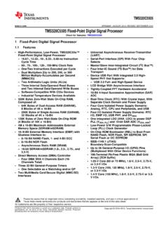
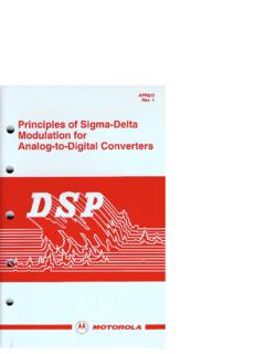
10 68 MSC8256 Six-Core Digital Signal Processor Data Sheet , Rev. 6 Freescale Semiconductor3 Figure 1. MSC8256 Block DiagramFigure 2. StarCore SC3850 DSP Subsystem Block DiagramJTAGRMUNote: The arrow direction indicates master or Interface 64/32-bit4 TDMsDMAI/O-InterruptConcentratorUARTC locksTimersResetSemaphoresOther DDRCLASS High-Speed Serial InterfaceModulesQUICCE ngine Four TDMs 256-Channels each4x GbaudBoot ROMI2 CVirtualInterruptsControllerSPIDMAS erialDMAS erial4x GbaudSix DSP Cores at 1 GHz or 800 MHzSGMIITw o S G M I IRGMII RGMIIM3 Memory1056 KbytePCI-EX 1x/2x/4xSubsystemDual RISC ProcessorsEthernetEthernetSPISC3850 DSP Core512 Kbyte32 Kbyte32 KbyteL1 ICacheL1 DCacheL2 Cache / M2 MemoryRapidIORapidIODDR Interface 64/32-bitDDRC ontrollerPCIExprSerDes 1 SerDes 2x2Tw o S G M I I32