Transcription of Operational Amplifier Circuits - MIT OpenCourseWare
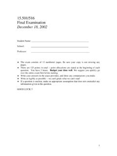
1 Operational Amplifier Circuits Review: Ideal Op-amp in an open loop configuration RoRi+_VpVnVi+_AViVo+IpIn An ideal op-amp is characterized with infinite open loop gain A The other relevant conditions for an ideal op-amp are: 1. 0 IpIn==2. Ri= 3. 0Ro= Ideal op-amp in a negative feedback configuration When an op-amp is arranged with a negative feedback the ideal rules are: 1. : input current constraint 0 IpIn==2. : input voltage constraint VnVp= These rules are related to the requirement/assumption for large open-loop gain , and they form the basis for op-amp circuit analysis. A The voltage Vn tracks the voltage Vp and the control of Vn is accomplished via the feedback network. Chaniotakis and Cory. Spring 2006 Page 1 Operational Amplifier Circuits as Computational Devices So far we have explored the use of op amps to multiply a signal by a constant.
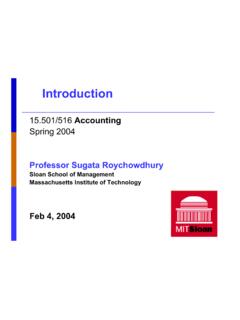
2 For the inverting Amplifier the multiplication constant is the gain 2R1R and for the non inverting Amplifier the multiplication constant is the gain 2RR11+. Op amps may also perform other mathematical operations ranging from addition and subtraction to integration, differentiation and We will next explore these fundamental Operational Circuits . Summing Amplifier A basic summing Amplifier circuit with three input signals is shown on Figure 1. R1 RFoutVin2VR2R3in1 Vin3V1I2I3 IFI1N Figure 1. Summing Amplifier Current conservation at node N1 gives 123 FIIII++= ( ) By relating the currents I1, I2 and I3 to their corresponding voltage and resistance by Ohm s law and noting that the voltage at node N1 is zero (ideal op-amp rule) Equation ( ) becomes 123123inininoutVVVVRRRRF++= ( ) 1 The term Operational Amplifier was first used by John Ragazzini et.
3 Al in a paper published in 1947. The relevant historical quotation from the paper is: As an Amplifier so connected can perform the mathematical operations of arithmetic and calculus on the voltages applied to its inputs, it is hereafter termed an Operational Amplifier . John Ragazzini, Robert Randall and Frederick Russell, Analysis of Problems in Dynamics by Electronics Circuits , Proceedings of IRE, Vol. 35, May 1947 Chaniotakis and Cory. Spring 2006 Page 2 And so Vout is 12122outinininRFRFRFVVVRRR = ++ 3V ( ) The output voltage Vout is a sum of the input voltages with weighting factors given by the values of the resistors. If the input resistors are equal R1=R2=R3=R, Equation ( ) becomes (123outinininRFVVV)VR= ++ ( ) The output voltage is thus the sum of the input voltages with a multiplication constant given by RFR.
4 The value of the multiplication constant may be varied over a wide range and for the special case when RF = R the output voltage is the sum of the inputs ()123outinininVVVV= ++ ( ) The input resistance seen by each source connected to the summing Amplifier is the corresponding series resistance connected to the source. Therefore, the sources do not interact with each other. Chaniotakis and Cory. Spring 2006 Page 3 Difference Amplifier This fundamental op amp circuit , shown on Figure 2, amplifies the difference between the input signals. The subtracting feature is evident from the circuit configuration which shows that one input signal is applied to the inverting terminal and the other to the non-inverting terminal.
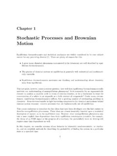
5 OutVin2 Vin1V1I2 IFI1NR2R1R3R4 Figure 2. Difference Amplifier Before we proceed with the analysis of the difference Amplifier let s think about the overall behavior of the circuit . Our goal is to obtain the difference of the two input signals()21-ininVV. Our system is linear and so we may apply superposition in order to find the resulting output. We are almost there once we notice that the contribution of the signal Vin2 to the output is 2241341outin2 RRVVRRR = + + ( ) and the contribution of signal Vin1 is 112-1outinRVVR = ( ) And the output voltage is 212142-1341outoutoutinin2-1 RRVVVVVRRRR ==+ + R ( ) Chaniotakis and Cory.
6 Spring 2006 Page 4 Note that in order to have a subtracting circuit which gives Vout=0 for equal inputs, the weight of each signal must be the same. Therefore 42134112 RRRRRR += + R ( ) which holds only if 4312 RRRR= ( ) The output voltage is now (212-1outininRVVV)R= ( ) which is a difference Amplifier with a differential gain of R2/R1 and with zero gain for the common mode signal. It is often practical to select resistors such as R4=R2 and R3=R1.
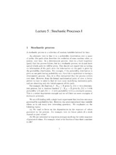
7 The fundamental problem of this circuit is that the input resistance seen by the two sources is not balanced. The input resistance between the input terminals A and B, the differential input resistance, Rid (see Figure 3) is inidRVI R1outV+VR2R3inVR4+-I-VAB Figure 3. Differential Amplifier Since V+ = V- , and thus 1 3 inVRIR=+I21idRR=. The desire to have large input resistance for the differential Amplifier is the main drawback for this circuit . This problem is addressed by the instrumentation Amplifier discussed next. Instrumentation Amplifier Figure 4 shows our modified differential Amplifier called the instrumentation Amplifier (IA). Op amps U1 and U2 act as voltage followers for the signals Vin1 and Vin2 which see the infinite input resistance of op amps U1 and U2.
8 Assuming ideal op amps, the voltage Chaniotakis and Cory. Spring 2006 Page 5 at the inverting terminals of op amps U1 and U2 are equal to their corresponding input voltages. The resulting current flowing through resistor R1 is 111ininVVI2R = ( ) Since no current flows into the terminals of the op amp, the current flowing through resistor R2 is also given by Equation ( ). in1 Vin2VR1R2R2R3R3R41V2V01V02 VoutVU1U2U3R4 Figure 4. Instrumentation Amplifier circuit Since our system is linear the voltage at the output of op-amp U1 and op-amp U2 is given by superposition as 01in1in222V1VV11 =+ RRRR ( ) 02in2in122V1VV11 =+ RRRR ( ) Next we see that op amp U3 is arranged in the difference Amplifier configuration examined in the previous section (see Equation ( )).
9 The output of the difference Amplifier is (outin2in1422V1VV31 =+ RRRR) ( ) The differential gain, 422131 RRRR + , may be varied by changing only one resistor: R1. Chaniotakis and Cory. Spring 2006 Page 6 Current to voltage converters A variety of transducers produce electrical current in response to an environmental condition. Photodiodes and photomultipliers are such transducers which respond to electromagnetic radiation at various frequencies ranging from the infrared to visible to -rays. A current to voltage converter is an op amp circuit which accepts an input current and gives an output voltage that is proportional to the input current. The basic current to voltage converter is shown on Figure 5.
10 This circuit arrangement is also called the transresistance Amplifier . inIRoutV1N Figure 5. Current to voltage converter Iin represents the current generated by a certain transducer. If we assume that the op amp is ideal, KCL at node N1 gives 100outoutV1 IVRR += = I ( ) The gain of this Amplifier is given by R. This gain is also called the sensitivity of the converter. Note that if high sensitivity is required for example 1V/ V then the resistance R should be 1 M . For higher sensitivities unrealistically large resistances are required. A current to voltage converter with high sensitivity may be constructed by employing the T feedback network topology shown on Figure 6.