Transcription of Optocoupler, Photodarlington Output, Dual Channel, SOIC-8 ...
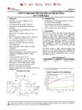
1 Document Number: 83648 For technical questions, contact: , 20-Apr-071 optocoupler , Photodarlington output , dual channel , SOIC-8 PackageILD223 TVishay SemiconductorsDESCRIPTIONThe ILD233T is a high current transfer ratio (CTR) optocoupler . It has a gallium arsenide infrared LED emitterand silicon NPN Photodarlington transistor device has CTRs tested at an LED current of low drive current permits easy interfacing from CMOS toLSTTL or ILD223T is constructed in a standard SOIC-8 foot printwhich makes it ideally suited for high density applications. Inaddition to eliminating through hole requirements, thispackage conforms to standards for surface Two channel optocoupler High current transfer ratio at IF = mA,500 % minimum Isolation test voltage, 4000 VRMS Electrical specifications similar to standard 6-pincoupler Compatible with dual wave, vapor phase and IR reflowsoldering SOIC-8 surface mountable package Standard lead spacing, " Available only on tape and reel (conforms to EIAstandard 481-2) Lead (Pb)-free component Component in accordance to RoHS 2002/95/EC andWEEE 2002/96/ECAGENCY APPROVALS UL1577, file no.
2 E52744 system code Y CUL - file no. E52744, equivalent to CSA bulletin 5A DIN EN 60747-5-2 (VDE 0884) available with option 1i179042A1C2A3C48C7E6C5 EORDER INFORMATIONPARTREMARKSILD223 TCTR > 500 %, SOIC-8 ABSOLUTE MAXIMUM RATINGS (1)PARAMETERTEST CONDITIONSYMBOLVALUEUNITINPUTPeak reverse pulsed s, 300 forward current per channel30mAPower dissipationPdiss45mWDerate linearly from 25 COUTPUTC ollector emitter breakdown voltageBVCEO30 VEmitter collector breakdown dissipation per channelPdiss75mWDerate linearly from 25 C technical questions, contact: Number: 836482 Rev. , 20-Apr-07 ILD223 TVishay SemiconductorsOptocoupler, Photodarlington output , dual channel , SOIC-8 PackageNotes(1)Tamb = 25 C, unless otherwise specifiedStresses in excess of the absolute maximum ratings can cause permanent damage to the device.
3 Functional operation of the device is notimplied at these or any other conditions in excess of those given in the operational sections of this document. Exposure to absolute maximumratings for extended periods of the time can adversely affect reliability.(2)Refer to reflow profile for soldering conditions for surface mounted devices (SOP/SOIC).NoteTamb = 25 C, unless otherwise specifiedMinimum and maximum values are testing requirements. Typical values are characteristics of the device and are the result of engineeringevaluation. Typical values are for information only and are not part of the testing test voltaget = sVISO4000 VRMST otal package dissipation(2 LEDs and 2 detectors, 2 channels)Ptot250mWDerate linearly from 25 CStorage temperature Tstg- 55 to + 150 COperating temperatureTamb- 55 to + 100 CSoldering temperature (2)Tsld260 CABSOLUTE MAXIMUM RATINGS (1)
4 PARAMETERTEST CONDITIONSYMBOLVALUEUNITELECTRICAL CHARACTERISTICSPARAMETERTEST voltageIF = 10 currentVR = ACapacitanceVF = 0 V, f = MHzCO25pFOUTPUTC ollector emitter breakdown voltageIC = 10 ABVCEO30 VEmitter collector breakdown voltageIC = 10 emitter leakage currentVCE = 50 V, IF = 0 AICEO50nACollector emitter capacitanceVCE = (input to output ) voltage, collector emitterIF = mA, ICE = , input to outputILD223 TCIO100G CURRENT TRANSFER RATIOPARAMETERTEST current transfer ratioIF = mA, VCE = VCTRDC500%SWITCHING CHARACTERISTICSPARAMETERTEST timeVCC = 10 V, RL = 100 , IF = mAILD223 Tton15 sTurn-off timeVCC = 10 V, RL = 100 , IF = mAILD223 Ttoff30 s Document Number: 83648 For technical questions, contact: , 20-Apr-073 ILD223 TOptocoupler, Photodarlington output , dual channel , SOIC-8 PackageVishay SemiconductorsNoteAs per IEC 60747-5-2, , this optocoupler is suitable for safe electrical insulation only within the safety ratings.
5 Compliance with thesafety ratings shall be ensured by means of prodective CHARACTERISTICSTamb = 25 C, unless otherwise specifiedFig. 3 - Forward Voltage vs. Forward CurrentFig. 4 - Peak LED Current vs. Duty Factor, Fig. 5 - Normalized CTRCE vs. LED CurrentFig. 6 - CTR vs. LED CurrentSAFETY AND INSULATION RATINGSPARAMETERTEST classification (according to IEC 68 part 1)55/100/21 Comparative tracking index CTI175399 VIOTM 6000 VVIORM560 VPSO 350mWISI 150mATSI 165 CCreepage distance4mmClearance distance4mmInsulation thickness, reinforced rated per IEC 60950 Forward Current (mA)VF- Forward Voltage (V)TA= - 55 CTA= 100 CTA= 25 Ciild223t_0210-610-510-410-310-210-11001 0110100100010000t - LED Pulse Duration (s)If(pk) - Peak LED Current (mA) Factort DF = /t CTRceTa = - 20 CTa = 25 CTa = 50 CTa = 70 CNormalized to:If = 1 mA, VCE = 5 VTa = 25 CTTamb = - 20 CTamb = 25 CTamb = 50 CTamb = 70 CNormalized to.
6 IF = 1 mA, VCE = 5 VTamb = 25 CIF - LED Current (mA) - Current Transfer Ratio (%)Tamb = - 20 CTamb = 25 CTamb = 50 CTamb = 70 CVCE = 5 VIF - LED Current (mA) technical questions, contact: Number: 836484 Rev. , 20-Apr-07 ILD223 TVishay SemiconductorsOptocoupler, Photodarlington output , dual channel , SOIC-8 PackageFig. 7 - Collector Current vs. LED CurrentFig. 8 - Switching SchematicFig. 9 - Switching TimingPACKAGE DIMENSIONS in inches (millimeters) - Collector Current (mA)Tamb = - 20 CTamb = 25 CTamb = 50 CTamb = 70 CVCE = 5 VIF - LED Current (mA)iild223t_06 VORLVCC= 10 VIF= 5 mAF = 10 kHz,DF = 50 %iild223t_07 IFtRVOtDtStFtPHLtPLHVTH= ( ) ( ) ( ) ( ) ( )R ( ) ( )i178020 ISO Method A40 ( ) ( ) ( ) ( ) ( )Lead coplanarity ( )7 ( ) ( ) ( )5 One ( ) ( ) ( ) ( )2 ( ) ( ) Document Number: 83648 For technical questions, contact.
7 , 20-Apr-075 ILD223 TOptocoupler, Photodarlington output , dual channel , SOIC-8 PackageVishay SemiconductorsOZONE DEPLETING SUBSTANCES POLICY STATEMENTIt is the policy of vishay Semiconductor GmbH to1. Meet all present and future national and international statutory Regularly and continuously improve the performance of our products, processes, distribution and operating systems withrespect to their impact on the health and safety of our employees and the public, as well as their impact on the is particular concern to control or eliminate releases of those substances into the atmosphere which are known as ozonedepleting substances (ODSs).The Montreal Protocol (1987) and its London Amendments (1990) intend to severely restrict the use of ODSs and forbid their usewithin the next ten years.
8 Various national and international initiatives are pressing for an earlier ban on these Semiconductor GmbH has been able to use its policy of continuous improvements to eliminate the use of ODSs listed inthe following Annex A, B and list of transitional substances of the Montreal Protocol and the London Amendments Class I and II ozone depleting substances in the Clean Air Act Amendments of 1990 by the Environmental Protection Agency(EPA) in the USA3. Council Decision 88/540/EEC and 91/690/EEC Annex A, B and C (transitional substances) Semiconductor GmbH can certify that our semiconductors are not manufactured with ozone depleting substances and donot contain such reserve the right to make changes to improve technical design and may do so without further can vary in different applications.
9 All operating parameters must be validated for each customer application by the customer. Should the buyer use vishay Semiconductors products for any unintended or unauthorized application, the buyer shall indemnify vishay Semiconductors against all claims, costs, damages, and expenses, arising out of, directly or indirectly, any claim of personal damage, injury or death associated with such unintended or unauthorized Semiconductor GmbH, 3535, D-74025 Heilbronn, GermanyLegal Disclaimer Revision: 08-Feb-171 Document Number: 91000 Disclaimer ALL PRODUCT, PRODUCT SPECIFICATIONS AND DATA ARE SUBJECT TO CHANGE WITHOUT NOTICE TO IMPROVE RELIABILITY, FUNCTION OR DESIGN OR OTHERWISE.
10 vishay Intertechnology, Inc., its affiliates, agents, and employees, and all persons acting on its or their behalf (collectively, vishay ), disclaim any and all liability for any errors, inaccuracies or incompleteness contained in any datasheet or in any other disclosure relating to any makes no warranty, representation or guarantee regarding the suitability of the products for any particular purpose or the continuing production of any product. To the maximum extent permitted by applicable law, vishay disclaims (i) any and all liability arising out of the application or use of any product, (ii) any and all liability, including without limitation special, consequential or incidental damages, and (iii) any and all implied warranties, including warranties of fitness for particular purpose, non-infringement and merchantability.