Transcription of Optocoupler, Phototransistor Output, Very High …
1 CNY64 AYST, CNY64 ABST, CNY64 AGRST, CNY65 AYST, CNY65 ABST, Semiconductors Rev. , 26-Jun-141 Document Number: 82387 For technical questions, contact: DOCUMENT IS SUBJECT TO CHANGE WITHOUT NOTICE. THE PRODUCTS DESCRIBED HEREIN AND THIS DOCUMENTARE SUBJECT TO SPECIFIC DISCLAIMERS, SET FORTH AT , Phototransistor output , very high Isolation VoltageDESCRIPTIONThe CNY6 XST, the high isolation voltage SMD version optocouplers consist of a Phototransistor optically coupled to a gallium arsenide infrared-emitting diode in a 4 pin plastic single components are mounted opposite one another, providing a distance between input and output for highest safety requirements of > 3 STANDARDST hese couplers perform safety functions according to the following equipment standards.
2 DIN EN 60747-5-5 (VDE 0884-5) optocoupler for electrical safety requirements IEC 60065 Safety for mains-operated electronic and related household apparatus VDE 0160 Electronic equipment for electrical power installationFEATURES Rated recurring peak voltage (repetitive) VIORM = 1450 Vpeak Thickness through insulation 3 mm Creepage current resistance according to VDE 0303/IEC 60112 comparative tracking index: CTI 475 Moisture sensitivity level MSL4- Follow defined storage and soldering requirements Material categorization: for definitions of compliance please see Solar and wind power diagnostic, monitoring, and communication equipment Welding equipment high voltage motors Switch-mode power supplies Line receiver Computer peripheral interface Microprocessor system interface Circuits for safe protective separation against electrical shock according to safety class II (reinforced isolation): - for appl.
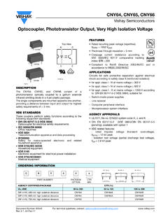
3 Class I to IV at mains voltage 300 V - for appl. class I to IV at mains voltage 600 V - for appl. class I to III at mains voltage 1000 V according to DIN EN 60747-5-5 (VDE 0884-5) AGENCY APPROVALS DIN EN 60747-5-5 (VDE 0884-5) UL1577, file no. E76222 VDE related features:- rated impulse voltage (transient overvoltage), VIOTM = 12 kVpeak- isolation test voltage (partial discharge test voltage), Vpd = kVpeakCEACTop View17187-5 VDE17187-6 CNY65 STCNY64 STORDERING INFORMATIONCNY6 #XXXSTPART NUMBERPACKAGE OPTIONCTR BINAGENCY CERTIFIED/PACKAGECTR (%)5 mAUL, VDE50 to 30050 to 15080 to 240100 to 300 SMD-4 HV, 400 mil high isolation distanceCNY64 STCNY64 AYSTCNY64 ABSTCNY64 AGRSTSMD-4 HV, 600 mil high isolation mmCNY64 STCNY65 STCNY64 AYST, CNY64 ABST, CNY64 AGRST, CNY65 AYST, CNY65 ABST, Semiconductors Rev.
4 , 26-Jun-142 Document Number: 82387 For technical questions, contact: DOCUMENT IS SUBJECT TO CHANGE WITHOUT NOTICE. THE PRODUCTS DESCRIBED HEREIN AND THIS DOCUMENTARE SUBJECT TO SPECIFIC DISCLAIMERS, SET FORTH AT Stresses in excess of the absolute maximum ratings can cause permanent damage to the device. Functional operation of the device is not implied at these or any other conditions in excess of those given in the operational sections of this document. Exposure to absolute maximum ratings for extended periods of the time can adversely affect Minimum and maximum values are testing requirements.
5 Typical values are characteristics of the device and are the result of engineering evaluation. Typical values are for information only and are not part of the testing MAXIMUM RATINGS (Tamb = 25 C, unless otherwise specified)PARAMETERTEST CONDITIONSYMBOLVALUEUNITINPUTR everse voltageVR5 VForward currentIF75mAForward surge currenttp 10 dissipationPdiss120mWJunction temperatureTj100 COUTPUTC ollector emitter voltageVCEO32 VEmitter collector voltageVECO7 VCollector currentIC50mACollector peak currenttp/T = , tp 10 msICM100mAPower dissipationPdiss130mWJunction temperatureTj100 CCOUPLERAC isolation test voltage CNY64 AxxxSTt = 1 isolation test voltage CNY65 AxxxSTt = 1 power dissipationPtot250mWAmbient temperature rangeTamb-55 to +85 CStorage temperature rangeTstg-55 to +100 CSoldering temperature2 mm from case.
6 10 sTsld260 CELECTRICAL CHARACTERISTICS (Tamb = 25 C, unless otherwise specified)PARAMETERTEST voltageIF = 50 capacitanceVR = 0 V, f = 1 MHzCj50pFOUTPUTC ollector emitter voltageIC = 1 mAVCEO32 VEmitter collector voltageIE = 100 AVECO7 VCollector emitter leakage currentVCE = 20 V, IF = 0 mAICEO200nACOUPLERC ollector emitter saturation voltageIF = 10 mA, IC = 1 frequencyVCE = 5 V, IF = 10 mA, RL = 100 fc110kHzCoupling capacitancef = 1 , CNY64 ABST, CNY64 AGRST, CNY65 AYST, CNY65 ABST, Semiconductors Rev. , 26-Jun-143 Document Number: 82387 For technical questions, contact: DOCUMENT IS SUBJECT TO CHANGE WITHOUT NOTICE.
7 THE PRODUCTS DESCRIBED HEREIN AND THIS DOCUMENTARE SUBJECT TO SPECIFIC DISCLAIMERS, SET FORTH AT According to DIN EN 60747-5-2 (see figure 2). This optocoupler is suitable for safe electrical isolation only within the safety ratings. Compliance with the safety ratings shall be ensured by means of suitable protective circuits. Fig. 1 - Safety Derating Diagram Fig. 2 - Test Pulse Diagram for Sample Test According to DIN EN 60747-5-2 (VDE 0884); IEC60747-5-5 CURRENT TRANSFER RATIO (Tamb = 25 C, unless otherwise specified)PARAMETERTEST = 5 V, IF = 5 mACNY64 STCTR50300%CNY65 STCTR50300%CNY64 AYSTCTR50150%CNY65 AYSTCTR50150%CNY64 ABSTCTR80240%CNY65 ABSTCTR80240%CNY64 AGRSTCTR100300%CNY65 AGRSTCTR100300%SAFETY AND INSULATION PARAMETERSPARAMETERTEST discharge test voltage - routine test100 %, ttest = 1 discharge test voltage - lot test (sample test)tTr = 60 s, ttest = 10 s,(see figure 2) resistanceVIO = 500 V, Tamb = 25 CRIO1012 VIO = 500 V, Tamb = 100 CRIO1011 VIO = 500 V, Tamb = 150 C(construction test only)
8 RIO109 Forward currentIsi120mAPower dissipationPso250mWRated impulse voltageVIOTM12kVSafety temperatureTsi150 CTracking resistance (comparative tracking index)Insulation group IVaCTI475 Minimum external tracking (creepage distance)Measured frominput pins to output pinsCNY64ST 14mm02550751001251501752002252500255075 100 125 150 175 200 Tamb ( C)22292 Pso (mW)Isi (mA)t13930t1, t2 = 1 s to 10 s t3, t4 = 1 s ttest = 10 s tstres = 12 s VIOTMVpdVIOWMVIORM0t1ttesttTr = 60 s tstrest3t4t2 CNY64 AYST, CNY64 ABST, CNY64 AGRST, CNY65 AYST, CNY65 ABST, Semiconductors Rev. , 26-Jun-144 Document Number: 82387 For technical questions, contact: DOCUMENT IS SUBJECT TO CHANGE WITHOUT NOTICE.
9 THE PRODUCTS DESCRIBED HEREIN AND THIS DOCUMENTARE SUBJECT TO SPECIFIC DISCLAIMERS, SET FORTH AT Fig. 3 - Test Circuit, Non-Saturated Operation Fig. 4 - Test Circuit, Saturated Operation Fig. 5 - Switching TimesSWITCHING CHARACTERISTICSPARAMETERTEST timeVS = 5 V, IC = 5 mA, RL = 100 , (see figure 3) sRise timeVS = 5 V, IC = 5 mA, RL = 100 , (see figure 3) sFall timeVS = 5 V, IC = 5 mA, RL = 100 , (see figure 3) sStorage timeVS = 5 V, IC = 5 mA, RL = 100 , (see figure 3) sTurn-on timeVS = 5 V, IC = 5 mA, RL = 100 , (see figure 3)ton5 sTurn-off timeVS = 5 V, IC = 5 mA, RL = 100 , (see figure 3)toff3 sTurn-on timeVS = 5 V, IF = 10 mA, RL = 1 k , (see figure 4)ton25 sTurn-off timeVS = 5 V, IF = 10 mA, RL = 1 k , (see figure 4)
10 SChannel I Channel II95 10900RG = 50 tptp = 50 s T= + 5 V IC = 5 mA; adjusted throughinput amplitudeIF0IF50100 OscilloscopeRL1 MCL20 pFChannel IChannel II95 10843RG= 50 tptp= 50 sT= + 5 VICIF050 1 k IF= 10 mAOscilloscopeRL CL20 pF 1 M tptt0010 %90 %100 %trtdtontstftoffIFICtpPulse durationtdDelay timetrRise timeton(= td + tr) Turn-on timetsStorage timetfFall timetoff(= ts + tf)Turn-off time96 11698 CNY64 AYST, CNY64 ABST, CNY64 AGRST, CNY65 AYST, CNY65 ABST, Semiconductors Rev. , 26-Jun-145 Document Number: 82387 For technical questions, contact: DOCUMENT IS SUBJECT TO CHANGE WITHOUT NOTICE. THE PRODUCTS DESCRIBED HEREIN AND THIS DOCUMENTARE SUBJECT TO SPECIFIC DISCLAIMERS, SET FORTH AT CHARACTERISTICS (Tamb = 25 C, unless otherwise specified) Fig.