Example: quiz answers
Packaging Material System for Electronic Devices
8 日立化成テクニカルレポートNo.40(2003-1) 総 説 ッケージングを行うWL(Wafer Level)-CSPが開発されてい る2 ),3 。 一方,チップとインタポーザの接続方法として現在
Tags:
Information
Domain:
Source:
Link to this page:
Documents from same domain
テクニカルレポート - hitachi-chem.co.jp
www.hitachi-chem.co.jp3 第 45 号 2005年7月 テクニカルレポート 巻頭言 わたしの研究の極意 5 山口由岐夫 論 文 リチウムイオン電池負極用バインダ樹脂 7
1 Abstract - hitachi-chem.co.jp
www.hitachi-chem.co.jpHitachi Chemical Technical Report No.58 18 3. Transmission characteristics of AS-400HS Evaluation results of transmission characteristics (transmission loss) of microstrip line of AS-400HS are shown in Figure 2.

Low Dielectric Constant Multilayer Material for …
www.hitachi-chem.co.jp日立化成テクニカルレポート no.57(2014・12月) 31 2.mcl-e-78gの一般特性 表1にmcl-e-78gの一般特性を示す。mcl-e-78gは1ghzで比誘電率(dk)3.5,誘電正接(df)0.011の誘電特性を有しており,
The balanced, reliable, advanced ... - hitachi …
www.hitachi-chem.co.jpGeneral Characteristics Item Condition Unit UL ANSI Multilayer Materials Multilayer Materials Materials For ICT Infrastructure *1) Heating Rate: 10℃/min. *2) Measured by Triplate-line Resonator *3)Cavity Resomator *4) 0.1mm *5) 0.2mm …

認定状況について - hitachi-chem.co.jp
www.hitachi-chem.co.jpul規格 bs規格・csa規格 電気用品安全法(cmj登録制度) 認定状況について p96 p98 p99 95

第 37 号 平成13年7月 ... - hitachi-chem.co.jp
www.hitachi-chem.co.jp3 第 37 号 平成13年7月 テクニカルレポート 巻頭言 光の風(高分子光部品の時代へ)─────────────────────────────────────────5
60 2017 - hitachi-chem.co.jp
www.hitachi-chem.co.jp日立化成 テクニカルレポート Hitachi Chemical Technical Report 第60号/2017.12 巻頭言 エネルギー事業のグローバル展開 ─ビジネスパートナーの真のニーズを捉える─ 4
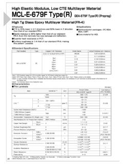
High Elastic Modulus, Low CTE ... - hitachi-chem.co.jp
www.hitachi-chem.co.jpCTE is 20% lower in X,Y directions and 50% lower in Z direction than that of our standard FR-4. Elastic modulus is 30% higher than that of our standard
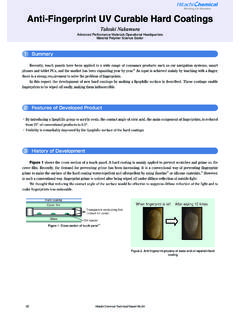
Anti-Fingerprint UV Curable Hard Coatings - …
www.hitachi-chem.co.jp37 Hitachi Chemical Technical Report No.54 Recently, touch panels have been applied to a wide range of consumer products such as car navigation systems, smart phones and tablet PCs, and the market has been expanding year by year.

日立機能性アクリレート メタクリレート
www.hitachi-chem.co.jp2 ファンクリル(fancryl)は、日立化成が開発した機能性アクリレート、メタクリレートの商品名です。 fa- a、fa- mの末尾の「a」はアクリレートを、「m」はメタクリレートを示しています。
Related documents

Development of Wafer-level Chip Size Package …
www.furukawa.co.jp古河電工時報第119号(平成19年1月) 14 一般論文 ウエハレベルチップサイズパッケージ(wl-csp)の開発

第 号 2003.1 テクニカルレポート
www.hitachi-chem.co.jp応力緩和型WL-CSPの外観写真 ウェハレベルCSP(Wafer Level Chip Size Pakage:WL-CSP)は,ウェハ状態で再配線や封止などの組立工程を行
YOLE DEVELOPPEMENT Advanced Packaging …
www.yole.frMainly supported today by flip-chip wafer bumping, the equipment market generated revenue of more than $930M in 2013. It is expected that this

Advanced IC Packaging as New Semiconductor …
theconfab.comAdvanced IC Packaging as New Semiconductor Industry Collaboration Platform CP Hung, Ph.D. VP of Corporate R&D ASE Inc. 25 Jun 2013
Orchestrating Packaging Technologies for an Extra …
www.semiconwest.orgOrchestrating Packaging Technologies for an Extra Sensory World Jean-Marc Yannou Christophe Zinck Eddie Cheng Vincent K. Liao Alex Chan Nicole Tien