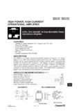
Transcription of PD-91279E IRF3205
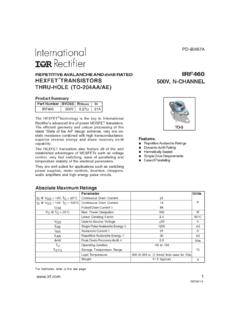
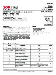
1 IRF3205 HEXFET Power MOSFET01/25/01 Absolute Maximum JCJunction-to-Case CSCase-to-Sink, Flat, Greased C/WR JAJunction-to-Ambient 62 Thermal = 55 VRDS(on) = ID = 110A SDGTO-220 ABAdvanced HEXFET Power MOSFETs from InternationalRectifier utilize advanced processing techniques to achieveextremely low on-resistance per silicon area. Thisbenefit, combined with the fast switching speed andruggedized device design that HEXFET power MOSFET sare well known for, provides the designer with an extremelyefficient and reliable device for use in a wide variety TO-220 package is universally preferred for allcommercial-industrial applications at power dissipationlevels to approximately 50 watts. The low thermalresistance and low package cost of the TO-220 contributeto its wide acceptance throughout the Process TechnologylUltra Low On-ResistancelDynamic dv/dt Ratingl175 C Operating TemperaturelFast SwitchinglFully Avalanche @ TC = 25 CContinuous Drain Current, VGS @ 10V 110 ID @ TC = 100 CContinuous Drain Current, VGS @ 10V 80 AIDMP ulsed Drain Current 390PD @TC = 25 CPower Dissipation200 WLinear Derating CVGSGate-to-Source Voltage 20 VIARA valanche Current 62 AEARR epetitive Avalanche Energy 20mJdv/dtPeak Diode Recovery dv/dt Junction and-55 to + 175 TSTGS torage Temperature RangeSoldering Temperature, for 10 seconds300 ( from case ) CMounting torque, 6-32 or M3 srew10 lbf in ( m) ParameterMin.
2 Typ. Max. Units ConditionsISContinuous Source CurrentMOSFET symbol(Body Diode) showing theISMP ulsed Source Currentintegral reverse(Body Diode) p-n junction Forward Voltage = 25 C, IS = 62A, VGS = 0V trrReverse Recovery Time 69104nsTJ = 25 C, IF = 62 AQrrReverse Recovery Charge 143215nCdi/dt = 100A/ s tonForward Turn-On TimeIntrinsic turn-on time is negligible (turn-on is dominated by LS+LD)Source-Drain Ratings and Characteristics110390A Starting TJ = 25 C, L = 138 H RG = 25 , IAS = 62A. (See Figure 12) Repetitive rating; pulse width limited by max. junction temperature. ( See fig. 11 )Notes: ISD 62A, di/dt 207A/ s, VDD V(BR)DSS, TJ 175 C Pulse width 400 s; duty cycle 2%.Electrical Characteristics @ TJ = 25 C (unless otherwise specified) Calculated continuous current based on maximum allowable junction temperature.
3 Package limitation current is Typ. Max. Units ConditionsV(BR)DSSD rain-to-Source Breakdown Voltage55 VVGS = 0V, ID = 250 A V(BR)DSS/ TJBreakdown Voltage Temp. Coefficient V/ C Reference to 25 C, ID = 1mARDS(on)Static Drain-to-Source On-Resistance VGS = 10V, ID = 62A VGS(th)Gate Threshold = VGS, ID = 250 AgfsForward Transconductance44 SVDS = 25V, ID = 62A 25 AVDS = 55V, VGS = 0V 250 VDS = 44V, VGS = 0V, TJ = 150 CGate-to-Source Forward Leakage 100 VGS = 20 VGate-to-Source Reverse Leakage -100nAVGS = -20 VQgTotal Gate Charge 146ID = 62 AQgsGate-to-Source Charge 35nCVDS = 44 VQgdGate-to-Drain ("Miller") Charge 54 VGS = 10V, See Fig. 6 and 13td(on)Turn-On Delay Time 14 VDD = 28 VtrRise Time 101 ID = 62 Atd(off)Turn-Off Delay Time 50 RG = tfFall Time 65 VGS = 10V, See Fig.
4 10 Between lead, 6mm ( )from packageand center of die contactCissInput Capacitance 3247 VGS = 0 VCossOutput Capacitance 781 VDS = 25 VCrssReverse Transfer Capacitance 211 pF = , See Fig. 5 EASS ingle Pulse Avalanche Energy 1050 264 mJIAS = 62A, L = 138 HnHLDI nternal Drain InductanceLSInternal Source Inductance Leakage Current This is a typical value at device destruction and represents operation outside rated limits. This is a calculated value limited to TJ = 175 2. Typical Output CharacteristicsFig 1. Typical Output CharacteristicsFig 3. Typical Transfer CharacteristicsFig 4. Normalized On-ResistanceVs. Temperature 1 10 100 1 10 10020 s PULSE WIDTHT = 25CJ , Drain-to-Source Voltage (V)I , Drain-to-Source Current (A) 1 10 100 1 10 10020 s PULSE WIDTHT = 175CJ , Drain-to-Source Voltage (V)I , Drain-to-Source Current (A) , Junction Temperature( C)R , Drain-to-Source On Resistance(Normalized)JDS(on) V=I=GSD10V107A 1 10 100 10004681012V = 25V20 s PULSE WIDTHDSV , Gate-to-Source Voltage (V)I , Drain-to-Source Current (A)GSDT = 25 CJ T = 175 CJ 7.
5 Typical Source-Drain DiodeForward VoltageFig 5. Typical Capacitance VoltageFig 6. Typical Gate Charge VoltageFig 7. Typical Source-Drain DiodeForward VoltageFig 8. Maximum Safe Operating Area110100 VDS, Drain-to-Source Voltage (V)0100020003000400050006000C, Capacitance(pF)CossCrssCissVGS = 0V, f = 1 MHZCiss = Cgs + Cgd, Cds SHORTEDCrss = Cgd Coss = Cds + Cgd0204060801001200246810121416Q , Total Gate Charge (nC)V , Gate-to-Source Voltage (V)GGSI=D62AV= 11 VDSV= 27 VDSV= 44 VDS 1 10 100 1000 10000 1 10 100 1000 OPERATION IN THIS AREA LIMITEDBY RDS(on) Single Pulse T T= 175 C= 25 C JCV , Drain-to-Source Voltage (V)I , Drain Current (A)I , Drain Current (A) 1 10 100 ,Source-to-Drain Voltage (V)I , Reverse Drain Current (A)SDSDV = 0 V GST = 25 CJ T = 175 CJ 9.
6 Maximum Drain Current TemperatureFig 10a. Switching Time Test CircuitVDS90%10%VGStd(on)trtd(off)tfFig 10b. Switching Time WaveformsFig 11. Maximum Effective Transient Thermal Impedance, Junction-to-CaseVDSP ulse Width 1 sDuty Factor % +-255075100125150175020406080100120T , Case Temperature( C)I , Drain Current (A) CDLIMITED BY PACKAGEFig 9. Maximum Drain Current TemperatureFig 10a. Switching Time Test CircuitVDS90%10%VGStd(on)trtd(off)tfFig 10b. Switching Time WaveformsFig 11. Maximum Effective Transient Thermal Impedance, Junction-to-CaseVDSP ulse Width 1 sDuty Factor % 1 Notes:1. Duty factor D =t / t2. Peak T=Px Z+ T12 JDMthJCC PttDM12t , Rectangular Pulse Duration (sec)Thermal Response(Z ) = PULSE(THERMAL RESPONSE) F50K .2 F12 VCurrent RegulatorSame Type as Sampling Resistors+-10 VFig 13b.
7 Gate Charge Test CircuitFig 13a. Basic Gate Charge WaveformFig 12b. Unclamped Inductive WaveformsFig 12a. Unclamped Inductive Test CircuittpV(BR)DSSIASFig 12c. Maximum Avalanche EnergyVs. Drain +-VDDDRIVERA15V20V2550751001251501750100 200300400500 Starting T , Junction Temperature( C)E , Single Pulse Avalanche Energy (mJ)JAS IDTOPBOTTOM25A 44A 62A Recoverydv/dtRipple 5%Body Diode Forward DropRe-AppliedVoltageReverseRecoveryCurr entBody Diode ForwardCurrentVGS=10 VVDDISDD river Gate VDSW aveformInductor CurentD = P. W .Period+-+++---Fig 14. For N-Channel HEXFETS* VGS = 5V for Logic Level DevicesPeak Diode Recovery dv/dt Test Circuit RGVDD dv/dt controlled by RG Driver same type as ISD controlled by Duty Factor "D" - Device Under Layout Considerations Low Stray Inductance Ground Plane Low Leakage Inductance Current Transformer * ASSIGNMENTS 1 - G A TE 2 - D R A IN 3 - SOURCE 4 - D R A IN- B (.)
8 052) (.048) (.022) (.018) (.115) (.104) (.185) (.165) (.037) (.027) (.160) (.140) (.045) M (.255) (.240) (.149) (.139)- A (.415) (.405) (.113) (.103) (.600) (.584) (.555) (.530) (.055) (.045) (.100) (.014) M B A M41 2 3 NOTES: 1 DIMENSIONING & TOLERANCING PER ANSI , 1982. 3 OUTLINE CONFORMS TO JEDEC OUTLINE TO-220AB. 2 CONTROLLING DIMENSION : INCH 4 HEATSINK & LEAD MEASUREMENTS DO NOT INCLUDE Marking InformationTO-220 ABPackage OutlineTO-220AB OutlineDimensions are shown in millimeters (inches)PART NUMBERINTERNATIONAL R ECTIFIER LO GOEXAMPLE : THIS IS AN IRF1010 W ITH ASSEMBLY L O T C O D E 9 B 1M ASSEMBLY L O T C O D EDATE CODE (YYW W )YY = YEARWW = WEEK9246IR F 10109B 1 MAData and specifications subject to change without notice.
9 This product has been designed and qualified for the automotive [Q101] Standards can be found on IR s Web WORLD HEADQUARTERS: 233 Kansas St., El Segundo, California 90245, USA Tel: (310) 252-7105 TAC Fax: (310) 252-7903 Visit us at for sales contact : For the most current drawings please refer to the IR website at.