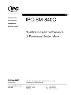
Transcription of Production Proven
1 3M Wafer Support SystemTemporary wafer bonding for advanced IC packaging High yields High throughput Cost effective Effectively handles wafers thinned to 20 mProductionProvenThe 3M Wafer Support System combines proprietary 3M temporary bonding technologies with world class equipment designed specifically to process wafers using 3M s wafer support system materials creating a complete, cost-effective solution for high-volume manufacturing of ultra-thin wafers for 3D TSV and related the 3M Wafer Support System worksThe heart of the system is 3M Liquid UV- curable Adhesive a family of 100% solids acrylic adhesives designed for temporary bonding of semiconductor wafers to a glass carrier plate. This provides a rigid, uniform support surface that minimizes stress on the wafer during the subsequent processing steps, resulting in less warpage, cracking, edge chipping and higher Wafer Support SystemA Production - Proven solution for increasing the capability, yields and throughput of your 3D TSV Flow (Bonding)Wafer is supporte d on t he entire face and the CarrierUV -Cured Liquid AdhesiveBackgrindLineLTHCR eleaseLayerWafer Reliablemanufacturingultra-thin wafer&EffectiveMore1 Bond2 Backgrinding3 Backside processing4 Tape application5 Laser debonding6 Glass Carrier Lift-off7 Peel off UV adhesive layer3M Liquid UV- curable Adhesive is spin-coated onto the wafer.
2 The wafer is then vacuum-bonded to the glass carrier, which has been treated with a release layer of 3M Light-To-Heat Conversion (LTHC) coating. During spin coating, the adhesive flows into the topography of the wafer front side, providing overall support even on large bump wafers. The system is designed to accommodate a single dispense and spin cycle on wafers with large 100 m features. Multiple spin and dr y cycles are not needed. As a liquid, it also provides more control over the Total Thickness Variation (TTV). The adhesive is then quickly cured with UV bonded wafer is thinned using standard backgrinding processes. The wafer is fully supported throughout the process, reducing edge cracking, chipping and thinning, the bonded wafer stack can be processed through standard semiconductor and TSV processes. 3M adhesives are designed to withstand high temperatures, of fer low outgassing in high vacuum semiconductor processes, and are resistant to typical process ter the wafer is processed, standard dicing tape is applied to the back of the wafer.
3 The wafer/glass carrier assembly is then placed in the debonding module, where it is suppor ted on a vacuum chuck for glass is separated from the adhesive using a laser debonding process. This is a low-stress process that utilizes no chemicals and is carried out at room laser processing the glass carrier is separated from the adhesive layer with very low force. The carrier is then recycled, allowing it to be re-used multiple Wafer De-Taping Tape 3305 is used to peel the UV adhesive from the wafer. Residue levels on the wafer surface after adhesive removal are minimal, comparable to conventional backgrinding tapes. No post-peel cleaning is required. Removal of the adhesive in this fashion also creates very lit tle stress to the thinned wafer, and is compatible with low-k -Cured Liquid AdhesiveWafer LTHC Release Layer Glass Carrier Grinding Wheel Making Cost Because it uses no wet chemistry or soaking steps to de-bond the carrier, the 3M Wafer Support System ( WSS ) offers fast and clean temporary wafer bonding and debonding.
4 And the 100% solids adhesive is recyclable, generating less waste by re-using the adhesive that does not remain on the wafer during the coating bonding and processing, a laser is used to debond the glass carrier, allowing easy, low force, chemical free separation of the support carrier from the adhesive surface. The adhesive is then peeled from the wafer using a simple peeling 3M Wafer Support System offers a Production - Proven and cost effective solution for handling wafers down to 20 microns during the backgrinding and subsequent high temperature 3D TSV FrameDicing TapeThinned WaferProcess Flow (Debonding)1 Bond2 Backgrinding3 Backside processing4 Tape application5 Laser debonding6 Glass Carrier Lift-off7 Peel off UV adhesive layer3M Liquid UV- curable Adhesive is spin-coated onto the wafer. The wafer is then vacuum-bonded to the glass carrier, which has been treated with a release layer of 3M Light-To-Heat Conversion (LTHC) coating.
5 During spin coating, the adhesive flows into the topography of the wafer front side, providing overall support even on large bump wafers. The system is designed to accommodate a single dispense and spin cycle on wafers with large 100 m features. Multiple spin and dr y cycles are not needed. As a liquid, it also provides more control over the Total Thickness Variation (TTV). The adhesive is then quickly cured with UV bonded wafer is thinned using standard backgrinding processes. The wafer is fully supported throughout the process, reducing edge cracking, chipping and thinning, the bonded wafer stack can be processed through standard semiconductor and TSV processes. 3M adhesives are designed to withstand high temperatures, of fer low outgassing in high vacuum semiconductor processes, and are resistant to typical process ter the wafer is processed, standard dicing tape is applied to the back of the wafer.
6 The wafer/glass carrier assembly is then placed in the debonding module, where it is suppor ted on a vacuum chuck for glass is separated from the adhesive using a laser debonding process. This is a low-stress process that utilizes no chemicals and is carried out at room laser processing the glass carrier is separated from the adhesive layer with very low force. The carrier is then recycled, allowing it to be re-used multiple Wafer De-Taping Tape 3305 is used to peel the UV adhesive from the wafer. Residue levels on the wafer surface after adhesive removal are minimal, comparable to conventional backgrinding tapes. No post-peel cleaning is required. Removal of the adhesive in this fashion also creates very lit tle stress to the thinned wafer, and is compatible with low-k to enable temporary bonding of wafers down to 20 microns with fast backgrinding speeds and high bonding of 3D TSV waferssolution forA complete Designed for semiconductor processes Compatible with high temperature/high vacuum processes, common process chemistries and low-k dielectric materials High yields Minimizes grinding and debonding stress for less warpage, cracking.
7 Edge chipping High throughput Uses no solvents and debonds at room temperature Less waste Overspray from spin coating can be captured and recycled3M s Wafer Support System combines 3M materials and Authorized WSS equipment to support temporary wafer bonding and ultra-thin wafer processing for 3D TSV processes and 3D packaging is partnering with some of the world s leading semiconductor equipment manufacturers to supply, service, and support the bonder, debonder, and glass recycling equipment used in the 3M Wafer Support Light-to-Heat-ConversionRelease CoatingGlass Carrier Customer-suppliedSemiconductor Wafer3M LC-SeriesLiquid UV- curable Adhesives3M Light-to-Heat-ConversionRelease CoatingGlass Carrier Customer-suppliedImportant Notice: Before using this product, you must evaluate it and determine if it is suitable for your intended application. You assume all risks and liability associated with such ; Limited Remedy; Limited Liability: 3M s product warranty is stated in its Product Literature available upon request.
8 3M MAKES NO OTHER WARRANTIES INCLUDING, BUT NOT LIMITED TO, ANY IMPLIED WARRANTY OF MERCHANTABILITY OR FITNESS FOR A PARTICULAR PURPOSE. If this product is defective within the warranty period stated above, your exclusive remedy shall be, at 3M s option, to replace or repair the 3M product or refund the purchase price of the 3M product. Except where prohibited by law, 3M will not be liable for any indirect, special, incidental or consequential loss or damage arising from this 3M product, regardless of the legal theory is a trademark of 3M Company. Used under license by 3M subsidiaries and af recycle. Printed in USA. 3M 2009. All rights : 12 / 09 6964HB60-5002-0049-2 Electronics Markets Materials Division3M Center, Building 225-3S-06St. Paul, MN 1-800-251-86343M Wafer Support System3M LC-Series Liquid UV- curable AdhesivesSemiconductor Wafer3M Wafer De-Taping Tape 33053M Wafer Support System MaterialsTemporary Bonding AdhesiveProduct NameBase ResinColorViscosityRecommended Application3M UV- curable Adhesive LC-3200 AcrylicClear, light yellow3500 CP @25 CLow-temps: 60+ min @ 150 C; several min @180 C*3M UV- curable Adhesive LC-4200 Acrylic, functional polymerClear, orange-brown2150 CP @25 CIntermediate temps: 90 min @ 180 C; several min @ 200 C*3M UV- curable Adhesive LC-5200 Acrylic, functional polymerClear, orange-brown~2000 CP @25 CHigh temps: 2 hrs @ 200 C; 1 hr @ 250 C + reflow cycles at 260 C** Thermal per formance varies by wafer construction.
9 Wafer evaluations should be used to validate per formance in LayerProduct NameCompositionColorFeatures3M Light-To-Heat-Conversion (LTHC) Release CoatingThermoplastic resinBlack in solution; semi-transparent grey as coatingAllows clean release of adhesive/glass bond upon laser irradiationAdhesive RemovalProduct NameBackingAdhesiveColorStandard Roll LengthTape ThicknessFeatures3M Wafer De-Taping Tape 3305 PolyesterRubberTranslucent cream100 meters (109 yards) mils ( mm)High instant adhesion. Allows for smooth unwind of view of WSS material layersBonding