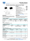
Transcription of Reflective Optical Sensor with Transistor Output
1 Semiconductors Rev. , 30-Jul-121 Document Number: 83751 For technical questions, contact: DOCUMENT IS SUBJECT TO CHANGE WITHOUT NOTICE. THE PRODUCTS DESCRIBED HEREIN AND THIS DOCUMENTARE SUBJECT TO SPECIFIC DISCLAIMERS, SET FORTH AT Optical Sensor with Transistor OutputDESCRIPTIONThe CNY70 is a Reflective Sensor that includes an infrared emitter and phototransistor in a leaded package which blocks visible Package type: leaded Detector type: phototransistor Dimensions (L x W x H in mm): 7 x 7 x 6 Peak operating distance: < mm Operating range within > 20 % relative collector current: 0 mm to 5 mm Typical Output current under test: IC = 1 mA Emitter wavelength.
2 950 nm Daylight blocking filter Lead (Pb)-free soldering released Material categorization: For definitions of compliance please see APPLICATIONS Optoelectronic scanning and switching devices , index sensing, coded disk scanning etc. (optoelectronic encoder assemblies).Notes(1)CTR: current transfere ratio, Iout/Iin(2)Conditions like in table basic charactristics/sensorsNote(1)MOQ: minimum order quantityEDTop viewMarking area19158_121835 PRODUCT SUMMARYPART NUMBERDISTANCE FOR MAXIMUM CTRrel (1)(mm)DISTANCE RANGE FORRELATIVE Iout > 20 %(mm)TYPICAL Output CURRENT UNDER TEST (2)(mA)DAYLIGHT BLOCKING FILTER INTEGRATEDCNY7000 to 51 YesORDERING INFORMATIONORDERING CODEPACKAGINGVOLUME (1)REMARKSCNY70 TubeMOQ.
3 4000 pcs, 80 pcs/tube-ABSOLUTE MAXIMUM RATINGS (Tamb = 25 C, unless otherwise specified)PARAMETERTEST CONDITIONSYMBOLVALUEUNITCOUPLERT otal power dissipationTamb 25 CPtot200mWAmbient temperature rangeTamb- 40 to + 85 CStorage temperature rangeTstg- 40 to + 100 CSoldering temperatureDistance to case 2 mm, t 5 sTsd260 CINPUT (EMITTER)Reverse voltageVR5 VForward currentIF50mAForward surge currenttp 10 sIFSM3 APower dissipationTamb 25 CPV100mWJunction temperatureTj100 C Semiconductors Rev. , 30-Jul-122 Document Number: 83751 For technical questions, contact: DOCUMENT IS SUBJECT TO CHANGE WITHOUT NOTICE. THE PRODUCTS DESCRIBED HEREIN AND THIS DOCUMENTARE SUBJECT TO SPECIFIC DISCLAIMERS, SET FORTH AT MAXIMUM RATINGSFig.
4 1 - Power Dissipation vs. Ambient TemperatureNotes(1)Measured with the Kodak neutral test card , white side with 90 % diffuse reflectance(2)Measured without reflecting mediumOUTPUT (DETECTOR)Collector emitter voltageVCEO32 VEmitter collector voltageVECO7 VCollector currentIC50mAPower dissipationTamb 25 CPV100mWJunction temperatureTj100 CABSOLUTE MAXIMUM RATINGS (Tamb = 25 C, unless otherwise specified)PARAMETERTEST CONDITIONSYMBOLVALUEUNIT0 100 200 300 095 11071P - Power Dissipation (mW) Tamb- Ambient Temperature ( C)IR - diodeCoupled device Phototransistor 255075100 BASIC CHARACTERISTICS (Tamb = 25 C, unless otherwise specified)PARAMETERTEST currentVCE = 5 V, IF = 20 mA, d = mm (figure 1)IC (2) talk currentVCE = 5 V, IF = 20 mA, (figure 2)ICX (3)600nACollector emitter saturation voltageIF = 20 mA, IC = mA, d = mm (figure 1)VCEsat (2) (EMITTER)Forward voltageIF = 50 intensityIF = 50 mA, tp = 20 wavelengthIF = 100 mA P940nmVirtual source diameterMethod: 63 % encircled (DETECTOR)Collector emitter voltageIC = 1 mAVCEO32 VEmitter collector voltageIE = 100 AVECO5 VCollector dark currentVCE = 20 V, IF = 0 A, E = 0 lxICEO200nA Semiconductors Rev.
5 , 30-Jul-123 Document Number: 83751 For technical questions, contact: DOCUMENT IS SUBJECT TO CHANGE WITHOUT NOTICE. THE PRODUCTS DESCRIBED HEREIN AND THIS DOCUMENTARE SUBJECT TO SPECIFIC DISCLAIMERS, SET FORTH AT 2 - Test ConditionBASIC CHARACTERISTICS (Tamb = 25 C, unless otherwise specified) Fig. 3 - Forward Current vs. Forward Voltage Fig. 4 - Relative Current Transfer Ratio vs. Ambient Temperature Fig. 5 - Collector Current vs. Forward Current Fig. 6 - Collector Current vs. Collector Emitter Voltage~~~~~~ACECD etectorEmitterd95 10893 Reflecting medium(Kodak neutral test card) - Forward Voltage (V)96 11862IF - Forward Current (mA) 96 11913 CTR - Relative Current Transfer Ratiorel T amb - Ambient Temperature ( C) - 30V = 5 V CEI = 20 mA Fd = mm 50403020100-10- 10 I - Collector Current (mA) C I F - Forward Current (mA) 95 11065 1 Kodak neutral card (white side) d = mmV CE= 5 V100 101 V CE- Collector Emitter Voltage (V)95 11066 I F = 50 mA20 mA10 mA5 mA 2 mA 1 mA 10 I - Collector Current (mA)C 1 Kodak neutral card (white side) d = mm100101 Semiconductors Rev.
6 , 30-Jul-124 Document Number: 83751 For technical questions, contact: DOCUMENT IS SUBJECT TO CHANGE WITHOUT NOTICE. THE PRODUCTS DESCRIBED HEREIN AND THIS DOCUMENTARE SUBJECT TO SPECIFIC DISCLAIMERS, SET FORTH AT Fig. 7 - Current Transfer Ratio vs. Forward Current Fig. 8 - Current Transfer Ratio vs. Collector Emitter Voltage Fig. 9 - Collector Current vs. Distance Fig. 10 - Relative Radiant Intensity/Collector Current Displacement Fig. 11 - Relative Collector Current vs. 1 10 100 I F - Forward Current (mA)96 11914 CTR - Current Transfer Ratio (%) Kodak neutral card (white side) d = mmV CE =5V 10010 1 1 10 V CE - Collector Emitter Voltage (V)96 12001 CTR - Current Transfer Ratio (%) 20 mA 10 mA 5 mA 2 mA 1 mAI F= 50 mA Kodak neutral card (white side) d = 110 100 0 1 10 I - Collector Current (mA)Cd - Distance (mm)95 11069 V CE = 5 VI F = 20 mAd 10 86 42 I - Relative Radiant Intensityerel95 11063 0 30 10 20 40 50 60 70 80 I - Relative Collector 0 0s - Displacement (mm)
7 96 11915 V CE= 5 VI F = 20 mAI - Relative Collector CurrentCrel d = 5 mm4 mm 3 mm 2 mm 1 mm 0 ED D E d s 0 5 mm 10 mm s 0 5 mm 10 mm 1110987654321 Semiconductors Rev. , 30-Jul-125 Document Number: 83751 For technical questions, contact: DOCUMENT IS SUBJECT TO CHANGE WITHOUT NOTICE. THE PRODUCTS DESCRIBED HEREIN AND THIS DOCUMENTARE SUBJECT TO SPECIFIC DISCLAIMERS, SET FORTH AT DIMENSIONS in millimetersTUBE DIMENSIONS in millimeters95 1134520291 Document Number: 80112 For technical questions, contact: , 02-Jul-091 Packaging and Ordering InformationPackaging and Ordering InformationVishay Semiconductors Notes(1)MOQ: minimum order quantity(2)Please refer to datasheetsTUBE SPECIFICATION FIGURESFig.
8 1 PART NUMBERMOQ (1)PCS PER TUBETUBE SPEC.(FIGURE)CONSTITUENTS(FORMS)CNY70400 080128 TCPT1300X012000 Reel(2)29 TCRT10001000 Bulk-26 TCRT10101000 Bulk-26 TCRT5000450050227 TCRT5000L240048327 TCST1030520065524 TCST1030L260065624 TCST1103102085424 TCST1202102085424 TCST1230480060724 TCST1300102085424 TCST2103102085424 TCST2202102085424 TCST2300102085424 TCST5250486030824 TCUT1300X012000 Reel(2)29 TCZT8020-PAER2500 Bulk-2215198 technical questions, contact: Number: 801122 Rev. , 02-Jul-09 Packaging and Ordering InformationVishay SemiconductorsPackaging and Ordering Information Fig. 2 Fig. 3 1521015201 Document Number: 80112 For technical questions, contact: , 02-Jul-093 Packaging and Ordering InformationPackaging and Ordering InformationVishay Semiconductors Fig.
9 4 Fig. 5 1519915202 technical questions, contact: Number: 801124 Rev. , 02-Jul-09 Packaging and Ordering InformationVishay SemiconductorsPackaging and Ordering Information Fig. 6 Fig. 7 1519615195 Document Number: 80112 For technical questions, contact: , 02-Jul-095 Packaging and Ordering InformationPackaging and Ordering InformationVishay Semiconductors Fig. 8 20257 Legal Disclaimer Revision: 01-Jan-20221 Document Number: 91000 Disclaimer ALL PRODUCT, PRODUCT SPECIFICATIONS AND DATA ARE SUBJECT TO CHANGE WITHOUT NOTICE TO IMPROVE RELIABILITY, FUNCTION OR DESIGN OR OTHERWISE. Vishay Intertechnology, Inc., its affiliates, agents, and employees, and all persons acting on its or their behalf (collectively, Vishay ), disclaim any and all liability for any errors, inaccuracies or incompleteness contained in any datasheet or in any other disclosure relating to any makes no warranty, representation or guarantee regarding the suitability of the products for any particular purpose or the continuing production of any product.
10 To the maximum extent permitted by applicable law, Vishay disclaims (i) any and all liability arising out of the application or use of any product, (ii) any and all liability, including without limitation special, consequential or incidental damages, and (iii) any and all implied warranties, including warranties of fitness for particular purpose, non-infringement and regarding the suitability of products for certain types of applications are based on Vishay's knowledge of typical requirements that are often placed on Vishay products in generic applications. Such statements are not binding statements about the suitability of products for a particular application.