Transcription of Single chip 2.4 GHz Transceiver ... - SparkFun Electronics
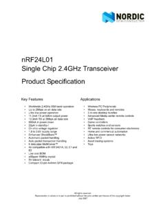
1 PRELIMINARY PRODUCT SPECIFICATION nordic Semiconductor ASA - Vestre Rosten 81, N-7075 Tiller, Norway - Phone +4772898900 - Fax +4772898989 Revision: Page 1 of 39 March 2006 Single chip GHz Transceiver FEATURES APPLICATIONS True Single chip GFSK Transceiver Wireless mouse, keyboard, joystick Complete OSI Link Layer in hardware Keyless entry Enhanced ShockBurst Wireless data communication Auto ACK & retransmit Alarm and security systems Address and CRC computation Home automation On the air data rate 1 or 2 Mbps Surveillance Digital interface (SPI) speed 0-8 Mbps Automotive 125 RF channel operation Telemetry Short switching time enable frequency hopping Intelligent sports equipment Fully RF compatible with nRF24XX Industrial sensors 5V tolerant signal input pads Toys 20-pin package (QFN20 4x4mm) Uses ultra low cost +/- 60 ppm crystal Uses low cost chip inductors and 2-layer PCB Power supply range: to V GENERAL DESCRIPTION nRF24L01 is a Single chip radio Transceiver for the world wide - GHz ISM band.
2 The Transceiver consists of a fully integrated frequency synthesizer, a power amplifier, a crystal oscillator, a demodulator, modulator and Enhanced ShockBurst protocol engine. Output power, frequency channels, and protocol setup are easily programmable through a SPI interface. Current consumption is very low, only at an output power of -6dBm and in RX mode. Built-in Power Down and Standby modes makes power saving easily realizable. QUICK REFERENCE DATA Parameter Value Unit Minimum supply voltage V Maximum output power 0 dBm Maximum data rate 2000 kbps Supply current in TX mode @ 0dBm output power mA Supply current in RX mode @ 2000 kbps mA Temperature range -40 to +85 C Sensitivity @ 1000 kbps -85 dBm Supply current in Power Down mode 900 nA Table 1 nRF24L01 quick reference data nRF24L01 PRELIMINARY PRODUCT SPECIFICATION nRF24L01 Single Chip GHz Radio Transceiver nordic Semiconductor ASA - Vestre Rosten 81, N-7075 Tiller.
3 Norway - Phone +4772898900 - Fax +4772898989 Revision: Page 2 of 39 March 2006 Type Number Description Version nRF24L01 20 pin QFN 4x4, RoHS & SS-00259 compliant D nRF24L01 IC Bare Dice D nRF24L01-EVKIT Evaluation kit (2 test PCB, 2 configuration PCB, SW) Table 2 nRF24L01 ordering information BLOCK DIAGRAM DVDDVDDVDDXC1XC2100+j175 IREFVDD_PA= VSS=0 VVDDVSS=0 VVSS=0 VFrequencySynthesiserPALNAIF BPFDEMODC lockRecovery,DataSlicerADDRD ecodeFIFOIn/Out CRCCode/DecodeEnhanced ShockBurstTMGFSKF ilterCSNMOSISCKVSS=0 VCEIRQMISO Figure 1 nRF24L01 with external components. PRELIMINARY PRODUCT SPECIFICATION nRF24L01 Single Chip GHz Radio Transceiver nordic Semiconductor ASA - Vestre Rosten 81, N-7075 Tiller, Norway - Phone +4772898900 - Fax +4772898989 Revision.
4 Page 3 of 39 March 2006 PIN FUNCTIONS Pin Name Pin function Description 1 CE Digital Input Chip Enable Activates RX or TX mode 2 CSN Digital Input SPI Chip Select 3 SCK Digital Input SPI Clock 4 MOSI Digital Input SPI Slave Data Input 5 MISO Digital Output SPI Slave Data Output, with tri-state option 6 IRQ Digital Output Maskable interrupt pin 7 VDD Power Power Supply (+3V DC) 8 VSS Power Ground (0V) 9 XC2 Analog Output Crystal Pin 2 10 XC1 Analog Input Crystal Pin 1 11 VDD_PA Power Output Power Supply (+ ) to Power Amplifier 12 ANT1 RF Antenna interface 1 13 ANT2 RF Antenna interface 2 14 VSS Power Ground (0V) 15 VDD Power Power Supply (+3V DC) 16 IREF Analog Input Reference current 17 VSS Power Ground (0V) 18 VDD Power Power Supply (+3V DC) 19 DVDD Power Output Positive Digital Supply output for de-coupling purposes 20 VSS Power Ground (0V) Table 3 nRF24L01 pin function PIN ASSIGNMENT nRF24L01 QFN20 4x4 VDDVSSANT2 VSSCE1920432115145 VDD_PAANT1121113 CSNMISOMOSIVDD18 IREFVSS1716 IRQDVDDVSS769108XC2XC1 VDDSCK Figure 2 nRF24L01 pin assignment (top view)
5 For a QFN20 4x4 package. PRELIMINARY PRODUCT SPECIFICATION nRF24L01 Single Chip GHz Radio Transceiver nordic Semiconductor ASA - Vestre Rosten 81, N-7075 Tiller, Norway - Phone +4772898900 - Fax +4772898989 Revision: Page 4 of 39 March 2006 ELECTRICAL SPECIFICATIONS Conditions: VDD = +3V, VSS = 0V, TA = - 40 C to + 85 C Symbol Parameter (condition) Notes Min. Typ. Max. Units Operating conditions VDD Supply voltage V TEMP Operating Temperature -40 +27 +85 C Digital input pin VIH HIGH level input voltage 1 V VIL LOW level input voltage VSS V Digital output pin VOH HIGH level output voltage (IOH= ) VDD- VDD V VOL LOW level output voltage (IOL= )
6 VSS V General RF conditions fOP Operating frequency 2 2400 2525 MHz fXTAL Crystal frequency 16 MHz f1M Frequency deviation @ 1000kbps 160 kHz f2M Frequency deviation @ 2000kbps 320 kHz RGFSK Data rate ShockBurst >0 2000 kbps FCHANNEL Channel spacing @ 1000kbps 1 MHz FCHANNEL Channel spacing @ 2000kbps 2 MHz Transmitter operation PRF Maximum Output Power 3 0 +4 dBm PRFC RF Power Control Range 16 18 20 dB PRFCR RF Power Accuracy 4 dB PBW 20dB Bandwidth for Modulated Carrier (2000kbps)
7 1800 2000 kHz PRF1 1st Adjacent Channel Transmit Power 2 MHz -20 dBm PRF2 2nd Adjacent Channel Transmit Power 4 MHz -50 dBm IVDD Supply current @ 0dBm output power 4 mA IVDD Supply current @ -18dBm output power mA IVDD Average Supply current @ -6dBm output power, Enhanced ShockBurst 5 mA IVDD Supply current in Standby-I mode 6 32 A IVDD Supply current in power down 900 nA 1 All digital inputs handle up to signal inputs.
8 Keep in mind that the VDD of the nRF24L01 must match the VIH of the driving device for output pins. 2 Usable band is determined by local regulations 3 Antenna load impedance = 15 +j88 4 Antenna load impedance = 15 +j88 . Effective data rate 1000kbps or 2000 kbps 5 Antenna load impedance = 15 +j88 . Effective data rate 10kbps and full packets 6 Given for a 12pF crystal. Current when using external clock is dependent on signal swing. PRELIMINARY PRODUCT SPECIFICATION nRF24L01 Single Chip GHz Radio Transceiver nordic Semiconductor ASA - Vestre Rosten 81, N-7075 Tiller, Norway - Phone +4772898900 - Fax +4772898989 Revision: Page 5 of 39 March 2006 Receiver operation IVDD Supply current one channel 2000kbps mA IVDD Supply current one channel 1000kbps mA RXSENS Sensitivity at (@2000kbps) -82 dBm RXSENS Sensitivity at (@1000kbps) -85 dBm C/ICO C/I Co-channel (@2000kbps) 7 78/119 dB C/I1ST 1st Adjacent Channel Selectivity C/I 2 MHz 1/4 dB C/I2ND 2nd Adjacent Channel Selectivity C/I 4 MHz -21/-20 dB C/I3RD 3rd Adjacent Channel Selectivity C/I 6 MHz -27/-27 dB C/ICO C/I Co-channel (@1000kbps)
9 10 911/1212 dB C/I1ST 1st Adjacent Channel Selectivity C/I 1 MHz 8/8 dB C/I2ND 2nd Adjacent Channel Selectivity C/I 2 MHz -22/-21 dB C/I3RD 3rd Adjacent Channel Selectivity C/I 3 MHz -30/-30 dB Table 4 nRF24L01 RF specifications 7 Data rate is 2000kbps for the following C/I measurements 8 According to ETSI EN 300 440-1 (2001-09) page 27 9 nRF24L01 equal modulation on interfering signal 10 Data rate is 1000kbps for the following C/I measurements 11 According to ETSI EN 300 440-1 (2001-09) page 27 12 nRF24L01 equal modulation on interfering signal PRELIMINARY PRODUCT SPECIFICATION nRF24L01 Single Chip GHz Radio Transceiver nordic Semiconductor ASA - Vestre Rosten 81, N-7075 Tiller, Norway - Phone +4772898900 - Fax +4772898989 Revision: Page 6 of 39 March 2006 PACKAGE OUTLINE nRF24L01 uses the QFN20 4x4 package, with matt tin plating.
10 PRELIMINARY PRODUCT SPECIFICATION nRF24L01 Single Chip GHz Radio Transceiver nordic Semiconductor ASA - Vestre Rosten 81, N-7075 Tiller, Norway - Phone +4772898900 - Fax +4772898989 Revision: Page 7 of 39 March 2006 Package Type A A1 A3 K D/E e D2/E2 L L1 b Saw QFN20 (4x4 mm) Min Typ. Max REF. min BSC13 BSC max Figure 3 nRF24L01 Package Outline. 13 BSC: Basic Spacing between Centers, ref. JEDEC standard 95, page PRELIMINARY PRODUCT SPECIFICATION nRF24L01 Single Chip GHz Radio Transceiver nordic Semiconductor ASA - Vestre Rosten 81, N-7075 Tiller, Norway - Phone +4772898900 - Fax +4772898989 Revision: Page 8 of 39 March 2006 Package marking: Abbreviations: B Build Code, unique code for production sites, package type and test platform X "X" grade, Engineering Samples (optional) YY 2 digit Year number WW 2 digit Week number LL 2 letter wafer lot number code Absolute Maximum Ratings Supply voltages VDD.
