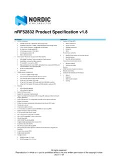
Transcription of nRF52832 - Nordic Semiconductor
1 All rights in whole or in part is prohibited without the prior written permission of the copyright - Product Specification 2 Contents1 Revision 92 About this Peripheral naming and Register 113 Block 124 Pin QFN48 pin 135 Absolute maximum 166 Recommended operating 177 Floating point Electrical CPU and support module RAM - Random access Flash - Non-volatile Memory 219 AHB AHB multilayer EasyDMA array 2511 NVMC Non-volatile memory Writing to Erasing a page in Writing to user information configuration registers (UICR).
2 Erasing user information configuration registers (UICR).. Erase Electrical 3012 BPROT Block 3113 FICR Factory information configuration 4114 UICR User information configuration 5215 Peripheral Peripheral Peripherals with shared Peripheral Bit set and 68 ContentsPage 316 Debug and DAP - Debug Access CTRL-AP - Control Access Debug interface Real-time 7317 Power and clock Current consumption 7418 POWER Power System OFF System ON Power supply RAM Retained Reset Electrical 9719 CLOCK Clock
3 HFCLK clock LFCLK clock Electrical 10520 GPIO General purpose Pin Notes on usage and Electrical 15121 GPIOTE GPIO tasks and Pin events and Port Tasks and events pin Electrical 16422 PPI Programmable peripheral Pre-programmed 16623 RADIO GHz Packet Maximum packet Address Data Radio Transmit Receive Received Signal Strength Indicator (RSSI).. Interframe Device address Bit Electrical 22624 TIMER Task Task Electrical 23725 RTC Real-time Clock Resolution versus overflow and the COUNTER Overflow TICK Event control Compare TASK and EVENT Reading the COUNTER Electrical 25026 RNG Random number Bias Electrical 25327 TEMP Temperature Electrical 25928 ECB AES electronic codebook mode Shared ECB data Electrical 26229 CCM AES CCM mode Shared AES CCM and RADIO
4 Concurrent Encrypting packets on-the-fly in radio transmit Decrypting packets on-the-fly in radio receive CCM data EasyDMA and ERROR 26830 AAR Accelerated address Shared Resolving a resolvable Use case example for chaining RADIO packet reception with address resolution IRK data Electrical 27631 SPIM Serial peripheral interface master with Shared SPI master transaction Low Master mode pin 280 ContentsPage Electrical 28632 SPIS Serial peripheral interface slave with Shared SPI slave Slave mode pin Electrical 29933 TWIM I2C compatible two-wire interface master with Shared Master write Master read Master repeated start Low Master mode pin Electrical 31334 TWIS I2C compatible two-wire interface slave with Shared TWI slave responding to a read TWI slave responding to a write Master repeated start Terminating an ongoing TWI Low Slave mode pin Electrical 32735 UARTE Universal asynchronous receiver/transmitter with Shared Error Using the UARTE without flow Parity Low Pin
5 Electrical 34136 QDEC Quadrature Sampling and LED Debounce Output/input Pin Electrical 35137 SAADC Successive approximation analog-to-digital Shared Digital Analog inputs and Operation Resistor Acquisition Limits event Electrical Performance 38638 COMP Shared Differential Single-ended Pin Electrical 39639 LPCOMP Low power Shared Pin Electrical 40440 WDT Watchdog Reload Temporarily pausing the Watchdog Electrical 41041 SWI Software 41142 NFCT Near field communication Pin Collision Frame timing Frame Frame Antenna NFCT antenna Battery Electrical 43143 PDM Pulse density modulation Master clock Module Decimation Hardware Pin Electrical 43944 I2S Inter-IC sound Transmitting and Left right clock (LRCK).
6 Serial clock (SCK).. Master clock (MCK).. 443 ContentsPage Width, alignment and Module Pin Electrical 45645 MWU Memory watch 45746 EGU Event generator Electrical 49047 PWM Pulse width Wave Decoder with Pin Electrical 50848 SPI Serial peripheral interface Functional Electrical 51449 TWI I2C compatible two-wire Functional Master mode pin Shared Master write Master read Master repeated start Low Electrical 52450 UART Universal asynchronous Functional Pin Shared Suspending the Error Using
7 The UART without flow Parity Electrical 53451 Mechanical QFN48 6 x 6 mm 53552 Ordering IC Box Order Code ranges and Product 53853 Reference Schematic QFAA QFN48 with internal LDO Schematic QFAA QFN48 with DC/DC regulator Schematic QFAA QFN48 with DC/DC regulator and NFC PCB PCB layout 54254 Liability Life support 5441 Revision historyPage 91 Revision historyDateVersionDescriptionFebruary About this documentPage 102 About this documentThis Product Specification is organized into chapters based on the modules and peripherals that areavailable in this peripheral descriptions are broken into separate sections that include the following information: A detailed functional description of the peripheral.
8 Register configuration for the peripheral Electrical specification tables providing the specified limits of the chip when tested under the conditionsdefined in the Recommended operating conditions on page Peripheral naming and abbreviationsEvery peripheral has a unique capitalized name or an abbreviation of its name, TIMER, used foridentification and reference. This name is used in chapter headings and references, and it will appear in theARM Cortex Microcontroller Software Interface Standard (CMSIS) hardware abstraction layer to identifythe peripheral instance name, which is different from the peripheral name, is constructed using theperipheral name followed by a numbered postfix, starting with 0, for example, TIMER0.
9 A postfix is normallyonly used if a peripheral can be instantiated more than once. The peripheral instance name is also used inthe CMSIS to identify the peripheral Register tablesIndividual registers are described using register tables. These tables are built up of two sections. The firstthree colored rows describe the position and size of the different fields in the register. The following rowsdescribe the fields in more Fields and valuesThe Id (Field Id) row specifies the bits that belong to the different fields in the blank space means that the field is reserved and that it is read as undefined, and must be written as 0 tosecure forward compatibility.
10 If a register is divided into more than one field, a unique field name is specifiedfor each field in the Field a field has enumerated values, then every value will be identified with a unique value id in the Value Idcolumn. Single-bit bit fields may, however, omit the Value Id when values can be substituted with a Booleantype enumerator range, for example, True/False, Disable/Enable, On/Off, and so are usually provided as decimal or hexadecimal. Hex values have a '0x' prefix, decimal values haveno Value column can be populated in the following ways: Individual enumerated values, for example, 1, 3, 9. Range of values, [ ], that is, all values from and including 0 and 4.
