Transcription of SMD - fpga4fun.com
1 INTERNATIONAL ATOMIC ENERGY AGENCYINSTRUMENTATION UNITSMD(SURFACE MOUNTED DEVICES) REPAIR1 SMD(SURFACE MOUNTED DEVICES)REPAIRS. WIERZBINSKIFEBRUARY 1999 INTERNATIONAL ATOMIC ENERGY AGENCYINSTRUMENTATION UNITSMD(SURFACE MOUNTED DEVICES) REPAIR2 TABLE OF CONTENTSPAGE1. INTRODUCTION32. SMD ADVANTAGES43. SMD LIMITATIONS44. SMD DIALECT55. SMD SIZES AND SMD CONSTRUCTION OF THE SMD marking OF THE SMD SMD SMD CERAMIC MULTILAYER CHIP SMD TANTALIUM SMD DIODES AND SMD INTEGRATED DIMENSIONS OF SO - , VSO - , PLCC - AND QFB - CASES16 INTERNATIONAL ATOMIC ENERGY AGENCYINSTRUMENTATION UNITSMD(SURFACE MOUNTED DEVICES) REPAIR31. INTRODUCTIONAt earlier eighties began a trend to replace a traditional through - hole technique with thesurface mounted technology (SMT) using surface mounted devices (SMD). The SMT, al-though intended in principle for automatic manufacturing only expand more and more, eveninto a hobby world.
2 This trend will continue, because many new components are available inSMD versions only. The SMT technique opens advantages and new applications throughminiaturising of the components and increasing of reliability. The industry standard unfortu-nately allows that most of the SMD components does not have a clear description. Since atiny size of the components they are labelled with a code. Therefore a sure identification ofthe components is impossible without appropriate technical documentation. Moreover thepolarity and pin - outs of different components could be not identified without data all of this factors is SMD for beginners a very hard brochure brings a help and clearance for a newcomer and moreover should help aservice technician to start a repair of the instruments made with the SMD components. Itpresents most of the SMD components available at the 1998 end with pin-outs and encodingcomparison tables: SMD / classic and classic / SMD.
3 The SMD does not present a newtechnique , it is only a miniaturisation of the components. But this components requires adifferent processing mounted devices (SMD) are active and passive electronics components withoutconventional connecting the conventional through - hole technology (THT) the components are placed on the components side of the printed circuit board (PCB), wires inserted into holes, and solderedto the copper pads on the opposite, solder side of the SMD components will be placed on the solder side of the PCB and their metal capssoldered to the copper pads of the PCB. Therefore both layers of the PCB could be used asactive areas. A thickness of PCBs used for SMD is between and mm. Historicallyroots of SMD are hybrid circuits on the ceramic substrates (middle of seventies) but a hugeindustrial applications of SMD started on a begin of the SMD does not stop. Distance between connection pins is reduced mm (past standard mm).
4 The winning standard for capacitors and resistors is 0402( x mm). The 0402 standard requires ten times less area then standard 1208 and fivetimes less then standard ATOMIC ENERGY AGENCYINSTRUMENTATION UNITSMD(SURFACE MOUNTED DEVICES) REPAIR42. SMD ADVANTAGES1. PCBs area much smaller then by conventional through - hole Since the both layers of the PCB could be used for assembling the final PCBs area forthe same circuits could be decreased by 50 %.3. Simple assembling - no bounding and cutting of the Automatic assembling very easy. Low cost of the Small size of components makes very high packing density possible. For the same cir-cuits a volume of a module assembled with SMD could be reduced to 30 % of the deviceassembled with the conventional technique. Therefore a size of the whole instrument de-crease, Very high resistance to mechanical shock and Low store and transport cost. Low store area and Lack of hole s drilling and Thin For great series low manufacturing SMD LIMITATIONSThe real goal of the SMD applications are a maximal packing density and finally volume re-duction of the modules and instruments.
5 Exactly this generates for which responsible are notthe SMD themselves, but the miniaturisation in Using ICs with a high amount of the pins (raster to mm, max. 148 pins) makesplacing of the paths between IC pins Design of SMD layout is very complex. Distances between soldering pads are fix. Di-mensions and distances between paths depends from soldering technology used High packing density brings thermal problems. Power dissipation of the power compo-nents is transferred directly through a copper layer of the PCB. The high temperature ofthe layer influence a neighbour Lack of the general SMD Not all SMD components are labelled with a clear text. Moreover, very often the compo-nents have no labels at Repair is more complex and difficult than by the conventional ATOMIC ENERGY AGENCYINSTRUMENTATION UNITSMD(SURFACE MOUNTED DEVICES) REPAIR54. SMD DIALECTSMD Surface Mounted Devices(active, passive and electromechanical components)SMT Surface Mounted Technology(assembling and montage technology)SMA Surface Mounted Technology(module assembled with SMT)SMD / CSurface Mounted Devices / Components(components for SMT)SMP Surface Mounted Packages(SMD case forms)SMES urface Mounted Equipment(SMT assembling machines)SO Small Outline(4 to 28 pins)VSO Very Small Outline(40 pins)SOP Small Outline Package(case)SOD Small Outline DiodeSOTS mall Outline TransistorSOICS mall Outline Integrated CircuitCCChip CarrierLCCL eadless Chip CarrierPLCCP lastic Leadless Chip CarrierLCCCL eadless Ceramic Chip CarrierMELFM etal Electrode Face BondingMINI MELFMini Metal Electrode Face BondingMICRO MELFM icro Metal Electrode Face BondingINTERNATIONAL ATOMIC ENERGY AGENCYINSTRUMENTATION UNITSMD(SURFACE MOUNTED DEVICES) REPAIR65.
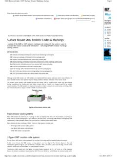
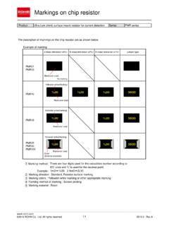
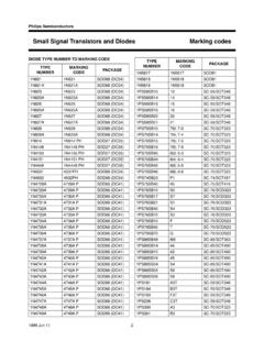
6 SMD SIZES AND DIMENSIONSThe coded description of the any SMD case form consists four digits which represents alength and a width in 1/100 ( mm). Length of the chipx x x xWidth of the chipEXAMPLE:Form mm x = mm x = SMD RESISTORST able Dimensions of the thick film chip resistorsFORMPOWER(Watt)LENGHT(mm)WIDTH( mm) ATOMIC ENERGY AGENCYINSTRUMENTATION UNITSMD(SURFACE MOUNTED DEVICES) REPAIR7 SMD resistors are available as a chip (rectangular form), or as a MELF (cylinder form). InSMT instead of the jumpers zero resistors are used. They are available in all standardSMD resistors dimensions and coded mostly with 000 .The most popular resistors case forms are 1206 (l = mm, w = mm, h = mm,Pmax = W by 70o) and 0805 (l = 2 mm, w = mm, Pmax = W by 70o).The rectangular chip forms are the same as for capacitors and could be processed by layoutdesign, assembling and repair with the same resistance values range is between 1 and 10 M and zero CONSTRUCTION OF THE SMD RESISTORSChip resistors are constructed with use of the thick film technique on a ceramic have metallic areas on the narrow ends of the chip, which allows soldering.
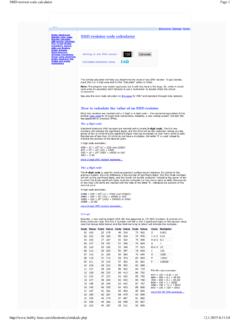
7 The resis-tive path is covered with a protective glaze. Chip resistors could be soldered with all commonsoldering techniques: reflow, wave and solder marking OF THE SMD RESISTORS5% and 2% SMD chip resistors are available in values according to IEC E 24 line andmarked with the following code:Table 5% and 2% resistors codeRESISTORIMPRINT0 (bridge) to XRX ( 9R1)10 to 91 XXR ( 91R)100 to 10 M See Table ATOMIC ENERGY AGENCYINSTRUMENTATION UNITSMD(SURFACE MOUNTED DEVICES) REPAIR8 Table Examples 4 7 3 A = 1st digit of the resistor s value B = 2nd digit of the resistor s value A B C C = number of zerosIMPRINTRESISTANCE VALUE101100 471470 1021 k k 10310 k 12312 k 104100 k 124120 k 474470 k 1% SMD chip resistors are coded with 3 - or 4 - digits. Available values in line E24 (E96).Table 1% resistor codeRESISTORIMPRINT100 to 988 XXXR1 k to 1 M XXXXT able Examples 4 7 3 2 A = 1st digit of the resistor s value B = 2nd digit of the resistor s value C = 3th digit of the resistor s value A B CD D = number of zerosIMPRINTRESISTANCE VALUE100R100 634R634 909R909 10011k k 100210 k 150215 k 54931549 k 10041 M MELF resistors are available in the three case forms:INTERNATIONAL ATOMIC ENERGY AGENCYINSTRUMENTATION UNITSMD(SURFACE MOUNTED DEVICES) REPAIR9 MELF form 0204, l= mm, d= mmMINIMELF form 0204, l= mm, d= mm MICROMELF form 0207, l= mm, d= mmResistance s value of the MELF resistors are marked with the standard 4 or 5 rings codeused by conventional resistors.
8 MELF resistors are available in IEC E24, E96 and E192lines, but not all tolerances are available. Zero resistors are available. Maximum load current is 2 A. The labels are 000 or 0R0 .Table International resistors colour code4-COLORS CODE5-COLORS CODE1 RING1 RING2 RING2 - 3 RING3 RING4 RING4 RING5 *100 -100k *47 -100k *10 -330k orange33000brown1%*1 yellow440000red2%*1 -10M green5500000gold5%* TRIMMPOTSSMD trimmpots are available in two different mechanical cases: three and four pins. Thefourth pin serves as a mechanical support only. The power dissipation of the SMD trimmpotis W. The slide could be turned a full angle of 360o, but active angle is 270o only. Therest 90o is a dead zone , where the slide has no contact to a resistance path. The value ofresistance vary between 100 and 1 M .INTERNATIONAL ATOMIC ENERGY AGENCYINSTRUMENTATION UNITSMD(SURFACE MOUNTED DEVICES) CERAMIC MULTILAYER CHIP CAPACITORSC eramic multilayer chip capacitors are available with a very wide range of values, from to 1 F.
9 This values are covered by seven cases forms. The forms depends of the ca-pacitors values. The most popular case are 0805 and 1206. Unfortunately this componentsare not marked, either with digital values, or colour code. This fact does not represent anyproblem for industry, where the components are assembled from the roll, but is very danger-ous for the service very careful with non-marked components! Avoid mixing them!Table Ceramic multilayer chip capacitors case forms. B L H ACASE FORML (mm)B (mm)H (mm)A (mm) to to to to to to to to to to to to ATOMIC ENERGY AGENCYINSTRUMENTATION UNITSMD(SURFACE MOUNTED DEVICES) SMD TANTALIUM CAPACITORSSMD tantalum capacitors are available in different case forms, partly without printedvalues. The + polarity is marked by white line, or white M . The case forms dependof capacitance value and nominal tantalum capacitors standard sizes are: x mm x mm x mm x mmThe values are coded with digits, or with alphanumerical WITH DIGITS: first position gives the first digit of the capacitance value second position gives the second digit of the capacitance value third position gives the number of zeros for value in pFEXAMPLE:Description 224 means 220 000 pF = 220 nF = FCODING WITH ALPHANUMERICAL CHARACTERS:CAPACITANCE CODECAPACITANCE(pF) VOLTAGE ATOMIC ENERGY AGENCYINSTRUMENTATION UNITSMD(SURFACE MOUNTED DEVICES) REPAIR121 F, 16 V.
10 CA* F, 35 V .. VJ* F, V ..JJ*+ C A G -NOMINALCAPACITANCEVOLTAGE2 EXAMPLE:A6 .. x 106 pF = FJ5 .. x 105 pF = FJ6 .. x 106 pF = FCAPACITANCE A 6+ - 3 5 VNOMINALVOLTAGEINTERNATIONAL ATOMIC ENERGY AGENCYINSTRUMENTATION UNITSMD(SURFACE MOUNTED DEVICES) SMD DIODES AND TRANSISTORSA lmost all standard diodes and transistors are available as SMD components inSOT - 23, SOT - 89 and SOT - 143 cases. In general electrical parameters of SMDdiodes and transistors are the same as comparable standard types in conventionalcases. SOT - 23, and SOT - 143 cases are used for components with power dissipa-tion 200 to 400 mW. SOT - 89 cases are used for power dissipation 500 mW to LEDs are available in SOT - 23 cases. All SMD transistors are marked SOT - xx casesINTERNATIONAL ATOMIC ENERGY AGENCYINSTRUMENTATION UNITSMD(SURFACE MOUNTED DEVICES) REPAIR14 Table Examples of SMD transistors -234 GBC860 CSOT -231F*MMBT5550 SOT -231F*BC847 BSOT -23AA*BCW60 ASOT -23AA*BCX51 SOT -89* HintThe same mark does not means the same component!