Transcription of SN54/74LS47 BCD TO 7-SEGMENT DECODER/DRIVER
1 SN54/74LS47 . BCD TO 7-SEGMENT . DECODER/DRIVER . The SN54 / 74LS47 are Low Power Schottky BCD to 7-SEGMENT Decod- er / drivers consisting of NAND gates, input buffers and seven AND-OR-IN- VERT gates. They offer active LOW, high sink current outputs for driving BCD TO 7-SEGMENT . indicators directly. Seven NAND gates and one driver are connected in pairs decoder / DRIVER. to make BCD data and its complement available to the seven decoding AND-OR-INVERT gates. The remaining NAND gate and three input buffers LOW POWER SCHOTTKY. provide lamp test, blanking input / ripple-blanking output and ripple-blanking input. The circuits accept 4-bit binary- coded -decimal (BCD) and, depending on the state of the auxiliary inputs, decodes this data to drive a 7-SEGMENT display indicator. The relative positive-logic output levels, as well as conditions required at the auxiliary inputs, are shown in the truth tables.
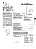
2 Output J SUFFIX. configurations of the SN54 / 74LS47 are designed to withstand the relatively CERAMIC. high voltages required for 7-SEGMENT indicators. CASE 620-09. These outputs will withstand 15 V with a maximum reverse current of 16. 1. 250 A. Indicator segments requiring up to 24 mA of current may be driven directly from the SN74LS47 high performance output transistors. Display patterns for BCD input counts above nine are unique symbols to authenticate input conditions. The SN54 / 74LS47 incorporates automatic leading and / or trailing-edge N SUFFIX. zero-blanking control (RBI and RBO). Lamp test (LT) may be performed at any PLASTIC. time which the BI / RBO node is a HIGH level. This device also contains an 16 CASE 648-08. overriding blanking input (BI) which can be used to control the lamp intensity 1. by varying the frequency and duty cycle of the BI input signal or to inhibit the outputs.
3 Lamp Intensity Modulation Capability (BI/RBO) D SUFFIX. Open Collector Outputs 16. SOIC. Lamp Test Provision 1 CASE 751B-03. Leading / Trailing Zero Suppression Input Clamp Diodes Limit High-Speed Termination Effects ORDERING INFORMATION. CONNECTION DIAGRAM DIP (TOP VIEW). SN54 LSXXJ Ceramic VCC f g a b c d e SN74 LSXXN Plastic 16 15 14 13 12 11 10 9 SN74 LSXXD SOIC. LOGIC SYMBOL. 7 1 2 6 3 5. 1 2 3 4 5 6 7 8. A B C D LT RBI. B C LT BI / RBO RBI D A GND. PIN NAMES LOADING (Note a). HIGH LOW BI/. a b c d e f g RBO. A, B, C, D BCD Inputs RBI Ripple-Blanking Input LT Lamp-Test Input 13 12 11 10 9 15 14 4. BI / RBO Blanking Input or Ripple-Blanking Output VCC = PIN 16. a, to g Outputs Open-Collector 15 ( ) GND = PIN 8. NOTES: a) 1 Unit Load ( ) = 40 A HIGH, mA LOW. b) Output current measured at VOUT = V. The Output LOW drive factor is for Military (54) and 15 for Commercial (74) Temperature Ranges.
4 FAST AND LS TTL DATA. 5-1. SN54/74LS47 . LOGIC DIAGRAM. a a A. b b B. INPUT. C c c D. OUTPUT. d d BLANKING INPUT OR. RIPPLE-BLANKING. OUTPUT e e f f LAMP-TEST. INPUT. RIPPLE-BLANKING. INPUT g g 0 1 2 3 4 5 6 7 8 9 10 11 12 13 14 15. NUMERICAL DESIGNATIONS RESULTANT DISPLAYS. TRUTH TABLE. INPUTS OUTPUTS. DECIMAL. OR LT RBI D C B A BI/RBO a b c d e f g NOTE. FUNCTION. 0 H H L L L L H L L L L L L H A. 1 H X L L L H H H L L H H H H A. 2 H X L L H L H L L H L L H L. 3 H X L L H H H L L L L H H L. 4 H X L H L L H H L L H H L L. 5 H X L H L H H L H L L H L L. 6 H X L H H L H H H L L L L L. 7 H X L H H H H L L L H H H H. 8 H X H L L L H L L L L L L L. 9 H X H L L H H L L L H H L L. 10 H X H L H L H H H H L L H L. 11 H X H L H H H H H L L H H L. 12 H X H H L L H H L H H H L L. 13 H X H H L H H L H H L H L L. 14 H X H H H L H H H H L L L L. 15 H X H H H H H H H H H H H H.
5 BI X X X X X X L H H H H H H H B. RBI H L L L L L L H H H H H H H C. LT L X X X X X H L L L L L L L D. H = HIGH Voltage Level L = LOW Voltage Level X = Immaterial NOTES: (A) BI/RBO is wire-AND logic serving as blanking Input (BI) and/or ripple-blanking output (RBO). The blanking out (BI) must be open or held at a HIGH level when output functions 0 through 15 are desired, and ripple-blanking input (RBI) must be open or at a HIGH level if blanking of a decimal 0 is not desired. X = input may be HIGH or LOW. (B) When a LOW level is applied to the blanking input (forced condition) all segment outputs go to a LOW level regardless of the state of any other input condition. (C) When ripple-blanking input (RBI) and inputs A, B, C, and D are at LOW level, with the lamp test input at HIGH level, all segment outputs go to a HIGH level and the ripple-blanking output (RBO) goes to a LOW level (response condition).
6 (D) When the blanking input/ripple-blanking output (BI/RBO) is open or held at a HIGH level, and a LOW level is applied to lamp test input, all segment outputs go to a LOW level. FAST AND LS TTL DATA. 5-2. SN54/74LS47 . GUARANTEED OPERATING RANGES. Symbol Parameter Min Typ Max Unit VCC Supply Voltage 54 V. 74 TA Operating Ambient Temperature Range 54 55 25 125 C. 74 0 25 70. IOH Output Current High BI / RBO 54, 74 50 A. IOL Output Current Low BI / RBO 54 mA. BI / RBO 74 VO (off) Off-State Output Voltage a to g 54, 74 15 V. IO (on) On-State Output Current a to g 54 12 mA. On-State Output Current a to g 74 24. DC CHARACTERISTICS OVER OPERATING TEMPERATURE RANGE (unless otherwise specified). Limits S b l Symbol P. Parameter Min Typ Max U i Unit T. Test C. Conditions di i Guaranteed Input HIGH Theshold Voltage VIH Input HIGH Voltage V. for All Inputs 54 Guaranteed Input p LOW Threshold Voltage g VIL Input LOW Voltage V.
7 74 for All Inputs VIK Input Clamp Diode Voltage V VCC = MIN, IIN = 18 mA. VCC = MIN,, IOH = 50 A, , VOH Output HIGH Voltage, Voltage BI / RBO 24. 42. V. VIN = VIN or VIL per Truth Table Output p LOW Voltage g 54, 74 V IOL = mA VCC = MIN,, VIN = VIN or VOL. BI / RBO 74 V IOL = mA VIL per Truth Table Off-State Output Current VCC = MAX, VIN = VIN or VIL per Truth IO (off) 250 A. a thru g Table, VO (off) = 15 V. On-State Output p Voltage g 54, 74 V IO (on) = 12 mA VCC = MAX, VIN = VIH. VO (on) or VIL per Truth T th Table T bl a thru g 74 V IO (on) = 24 mA. 20 A VCC = MAX, VIN = V. IIH Input HIGH Current mA VCC = MAX, VIN = V. Input LOW Current BI / RBO IIL mA VCC = MAX, VIN = V. Any Input except BI / RBO IOS BI / RBO Output Short Circuit Current (Note 1) mA VCC = MAX, VOUT = 0 V. ICC Power Supply Current 13 mA VCC = MAX. Note 1: Not more than one output should be shorted at a time, nor for more than 1 second.
8 AC CHARACTERISTICS (TA = 25 C). Limits Symbol S b l Parameter P Min Typ Max Unit U i Test T Conditions C di i tPHL Propagation Delay, Address 100 ns tPLH Input to segment Output 100 ns VCC = V. tPHL Propagation Delay, RBI Input 100 ns CL = 15 pF. tPLH To segment Output 100 ns AC WAVEFORMS. VIN V V VIN V V. tPHL tPLH tPHL tPLH. VOUT V V VOUT V V. Figure 1 Figure 2. FAST AND LS TTL DATA. 5-3.