Transcription of Spartan-3AN FPGA Family Data Sheet (DS557)
1 DS557 June 12, Specification1 Copyright 2007 2014 xilinx , Inc. xilinx , the xilinx logo, Artix, ISE, Kintex, Spartan, Virtex, Vivado, Zynq, and other designated brands included herein are trademarks of xilinx in the United States and other countries. PCI and PCI-X are trademarks of PCI-SIG and used under license. All other trademarks are the property of their respective 1: Introduction and Ordering InformationDS557 ( ) June 12, 2014 Introduction Features Architectural Overview Configuration Overview In-system Flash Memory Overview General I/O Capabilities Supported Packages and Package Marking Ordering InformationModule 2: Functional DescriptionDS557 ( ) June 12, 2014 The functionality of the Spartan -3AN FPGA Family is described in the following documents: UG331: Spartan-3 Generation FPGA User Guide Clocking Resources Digital Clock Managers (DCMs) Block RAM Configurable Logic Blocks (CLBs)-Distributed RAM-SRL16 Shift Registers-Carry and Arithmetic Logic I/O Resources Embedded Multiplier Blocks Programmable Interconnect ISE Design Tools and IP Cores Embedded Processing and Control Solutions Pin Types and Package Overview Package Drawings Powering FPGAs Power Management UG332.
2 Spartan-3 Generation Configuration User Guide Configuration Overview Configuration Pins and Behavior Bitstream Sizes Detailed Descriptions by Mode-Self-contained In-System Flash mode-Master Serial Mode using Platform Flash PROM-Master SPI Mode using Commodity Serial Flash-Master BPI Mode using Commodity Parallel Flash-Slave Parallel (SelectMAP) using a Processor-Slave Serial using a Processor-JTAG Mode ISE iMPACT Programming Examples MultiBoot Reconfiguration Design Authentication using Device DNA UG333: Spartan-3AN In-System Flash User Guide UG334: Spartan-3AN Starter Kit User GuideModule 3: DC and Switching CharacteristicsDS557 ( ) June 12, 2014 DC Electrical Characteristics Absolute Maximum Ratings Supply Voltage Specifications Recommended Operating Conditions Switching Characteristics I/O Timing Configurable Logic Block (CLB) Timing Multiplier Timing Block RAM Timing Digital Clock Manager (DCM) Timing Suspend Mode Timing Device DNA Timing Configuration and JTAG TimingModule 4: Pinout DescriptionsDS557 ( ) June 12, 2014 Pin Descriptions Package Overview Pinout Tables Footprint DiagramsAdditional information on the Spartan-3AN Family can be found at: FPGA Family Data SheetDS557 June 12, 2014 Product SpecificationTable 1:Production Status of Spartan-3AN FPGAsSpartan-3AN FPGAS tatusXC3S50 ANProductionXC3S200 ANProductionXC3S400 ANProductionXC3S700 ANProductionXC3S1400 ANProductionDS557 ( ) June 12, Specification2 Copyright 2007 2014 xilinx , Inc.
3 xilinx , the xilinx logo, Artix, ISE, Kintex, Spartan, Virtex, Vivado, Zynq, and other designated brands included herein are trademarks of xilinx in the United States and other countries. PCI and PCI-X are trademarks of PCI-SIG and used under license. All other trademarks are the property of their respective Spartan -3AN FPGA Family combines the best attributes of a leading edge, low cost FPGA with nonvolatile technology across a broad range of densities. The Family combines all the features of the Spartan-3A FPGA Family plus leading technology in-system Flash memory for configuration and nonvolatile data Spartan-3AN FPGAs are part of the Extended Spartan-3A Family , which also includes the Spartan-3A FPGAs and the higher density Spartan-3A DSP FPGAs. The Spartan-3AN FPGA Family is excellent for space-constrained applications such as blade servers, medical devices, automotive infotainment, telematics, GPS, and other small consumer products. Combining FPGA and Flash technology minimizes chip count, PCB traces and overall size while increasing system Spartan-3AN FPGA internal configuration interface is completely self-contained, increasing design security.
4 The Family maintains full support for external configuration. The Spartan-3AN FPGA is the world s first nonvolatile FPGA with MultiBoot, supporting two or more configuration files in one device, allowing alternative configurations for field upgrades, test modes, or multiple system The new standard for low cost nonvolatile FPGA solutions Eliminates traditional nonvolatile FPGA limitations with the advanced 90 nm Spartan-3A device feature set Memory, multipliers, DCMs, SelectIO, hot swap, power management, etc. Integrated robust configuration memory Saves board space Improves ease-of-use Simplifies design Reduces support issues Plentiful amounts of nonvolatile memory available to the user Up to 11+ Mb available MultiBoot support Embedded processing and code shadowing Scratchpad memory Robust 100K Flash memory program/erase cycles 20 years Flash memory data retention Security features provide bitstream anti-cloning protection Buried configuration interface Unique Device DNA serial number in each device for design Authentication to prevent unauthorized copying Flash memory sector protection and lockdown Configuration watchdog timer automatically recovers from configuration errors Suspend mode reduces system power consumption Retains all design state and FPGA configuration data Fast response time, typically less than 100 s Full hot-swap compliance Multi-voltage.
5 Multi-standard SelectIO interface pins Up to 502 I/O pins or 227 differential signal pairs LVCMOS, LVTTL, HSTL, and SSTL single-ended signal standards , , , , and signaling Up to 24 mA output drive 10% compatibility and hot swap compliance 622+ Mb/s data transfer rate per I/O DDR/DDR2 SDRAM support up to 400 Mb/s LVDS, RSDS, mini-LVDS, PPDS, and HSTL/SSTL differential I/O Abundant, flexible logic resources Densities up to 25,344 logic cells Optional shift register or distributed RAM support Enhanced 18 x 18 multipliers with optional pipeline Hierarchical SelectRAM memory architecture Up to 576 Kbits of dedicated block RAM Up to 176 Kbits of efficient distributed RAM Up to eight Digital Clock Managers (DCMs) Eight global clocks and eight additional clocks per each half of device, plus abundant low-skew routing Complete xilinx ISE and WebPACK software development system support MicroBlaze and PicoBlaze embedded processor cores Fully compliant 32-/64-bit 33 MHz PCI technology support Low-cost QFP and BGA Pb-free (RoHS) packaging options Pin-compatible with the same packages in the Spartan-3A FPGA family9 Spartan-3AN FPGA Family :Introduction and Ordering InformationDS557 ( ) June 12, 2014 Product SpecificationTa b l e 2.
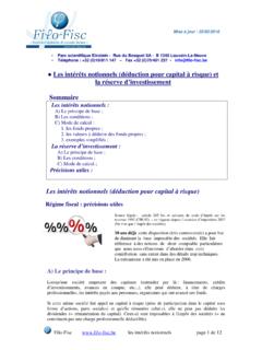
6 Summary of Spartan-3AN FPGA AttributesDeviceSystem GatesEquivalent Logic Cells CLBs SlicesDistributedRAM Bits(1)Block RAM Bits(1)Dedicated Multipliers DCMsMaximum User I/OMax Differential I/O PairsBitstream Size(1)In-System Flash BitsXC3S50AN50K1,58417670411K54K32108504 27K1M(2)XC3S200AN200K4,0324481,79228K288 K164195901,168K4 MXC3S400AN400K8,0648963,58456K360K204311 1421,842K4 MXC3S700AN700K13,2481,4725,88892K360K208 3721652,669K8 MXC3S1400AN 1400K25,3442,816 11,264176K576K3285022274,644K16 MNotes: convention, one Kb is equivalent to 1,024 bits and one Mb is equivalent to 1,024 supported by xilinx tools. See the customer notice XCN14003: Flash Wafer Fabrication Change and Gold (Au) To Copper (Cu) Transition for Spartan-3AN FPGA FPGA Family : Introduction and Ordering InformationDS557 ( ) June 12, Specification3 Architectural OverviewThe Spartan-3AN FPGA architecture is compatible with that of the Spartan-3A FPGA. The architecture consists of five fundamental programmable functional elements: Configurable Logic Blocks (CLBs) contain flexible Look-Up Tables (LUTs) that implement logic plus storage elements used as flip-flops or latches.
7 Input/Output Blocks (IOBs) control the flow of data between the I/O pins and the internal logic of the device. IOBs support bidirectional data flow plus 3-state operation. They support a variety of signal standards, including several high-performance differential standards. Double Data-Rate (DDR) registers are included. Block RAM provides data storage in the form of 18-Kbit dual-port blocks. Multiplier Blocks accept two 18-bit binary numbers as inputs and calculate the product. Digital Clock Manager (DCM) Blocks provide self-calibrating, fully digital solutions for distributing, delaying, multiplying, dividing, and phase-shifting clock elements are organized as shown in Figure 1. A dual ring of staggered IOBs surrounds a regular array of CLBs. Each device has two columns of block RAM except for the XC3S50AN, which has one column. Each RAM column consists of several 18-Kbit RAM blocks. Each block RAM is associated with a dedicated multiplier. The DCMs are positioned in the center with two at the top and two at the bottom of the device.
8 The XC3S50AN has DCMs only at the top, while the XC3S700AN and XC3S1400AN add two DCMs in the middle of the two columns of block RAM and Spartan-3AN FPGA features a rich network of traces that interconnect all five functional elements, transmitting signals among them. Each functional element has an associated switch matrix that permits multiple connections to the Target - Figure 1 Figure 1: Spartan-3AN Family ArchitectureCLBB lock RAMM ultiplierDCMIOBsIOBsDS557-1_01_122006 IOBsIOBsDCMB lock RAM / MultiplierDCMCLBsIOBsOBsDCMN otes: XC3S700AN and XC3S1400AN have two additional DCMs on both the left and right sides as indicated by the dashed lines. The XC3S50AN has only two DCMs at the top and only one Block RAM/Multiplier FPGA Family : Introduction and Ordering InformationDS557 ( ) June 12, Specification4 ConfigurationSpartan-3AN FPGAs are programmed by loading configuration data into robust, reprogrammable, static CMOS configuration latches (CCLs) that collectively control all functional elements and routing resources.
9 The FPGA s configuration data is stored on-chip in nonvolatile Flash memory, or externally in a PROM or some other nonvolatile medium, either on or off the board. After applying power, the configuration data is written to the FPGA using any of seven different modes: Configure from internal SPI Flash memory (Figure 2) Completely self-contained Reduced board space Easy-to-use configuration interface Master Serial from a xilinx Platform Flash PROM Serial Peripheral Interface (SPI) from an external industry-standard SPI serial Flash Byte Peripheral Interface (BPI) Up from an industry-standard x8 or x8/x16 parallel NOR Flash Slave Serial, typically downloaded from a processor Slave Parallel, typically downloaded from a processor Boundary-Scan (JTAG), typically downloaded from a processor or system testerThe MultiBoot feature stores multiple configuration files in the on-chip Flash, providing extended life with field upgrades. MultiBoot also supports multiple system solutions with a single board to minimize inventory and simplify the addition of new features, even in the field.
10 Flexibility is maintained to do additional MultiBoot configurations via the external configuration Spartan-3AN device authentication protocol prevents cloning. Design cloning, unauthorized overbuilding, and complete reverse engineering have driven device security requirements to higher and higher levels. Authentication moves the security from bitstream protection to the next generation of design-level security protecting both the design and embedded microcode. The authentication algorithm is entirely user defined, implemented using FPGA logic. Every product, generation, or design can have a different algorithm and functionality to enhance Flash MemoryEach Spartan-3AN FPGA contains abundant integrated SPI serial Flash memory, shown in Ta b l e 3, used primarily to store the FPGA s configuration bitstream. However, the Flash memory array is large enough to store at least two MultiBoot FPGA configuration bitstreams or nonvolatile data required by the FPGA application, such as code-shadowed MicroBlaze processor configuration, the FPGA design has full access to the in-system Flash memory via an internal SPI interface; the control logic is implemented with FPGA logic.