Example: bankruptcy
반도체 나노 패터닝 구현 재료: Spin 코팅 Hardmask용 …
472 Polymer Science and Technology Vol. 20, No. 5, October 2009 1. 서론 1.1 미세 패터닝을 위한 Hardmask의 필요성 및 공정 반도체 선폭이 미세화됨에 따라, 특히 70 nm 이하의 패턴을 구현함 에 있어, 기존처럼 두꺼운 두께(>300 nm)의 photoresist(PR)를 사
Information
Domain:
Source:
Link to this page:
Documents from same domain
차세대 투명전극 소재의 종류와 특성 - cheric.org
www.cheric.org244 정문현⋅김세열⋅유도혁⋅김중현 공업화학, 제25 권 제3 호, 2014 (a) (b) Figure 2. (a) Schematic of graphene transfer process[14], (b) Graphene
GPC 분석에서 중요한 핵심포인트들 - cheric.org
www.cheric.org556 Polymer Science and Technology Vol. 19, No. 6, December 2008 1. 서론 고분자의 분자량 측정은 우리가 신체 검사시 제일 먼저 키와 몸무 게를 재는 것과 같이 고분자분야에서 가장 기본적이고 중요한 분석중
터치 스크린 패널용 광학 접착소재 - cheric.org
www.cheric.org일반총설 | 터치 스크린 패널용 광학 접착소재 314 Polymer Science and Technology Vol. 26, No. 4, August 2015 그림 1. TSP의 시장 전망.1 …
주사전자현미경의 기본원리와 응용(Part Ⅱ
www.cheric.org주사전자현미경의 기본원리와 응용(Part Ⅱ) KIC News, Volume 13, No. 1, 2010 53 Figure 3. 전자총 외부, Wehnelt 실린더, 텅스턴 필라멘트 사진.
Modified Soave-Redlich-Kwong Equations of State Applied …
www.cheric.orgThe Soave-Redlich-Kwong EoS (SRK) is probably the most wide- ly employed model to correlate and predict fluid properties and phase equilibria in the process industry.

Introduction to Safety in Chemical Process Industry
www.cheric.orgPetrochemicals, "Black Gold, Texas Tea": Form many useful products from petroleum by developing processes like catalytic cracking gasoline, lubricating oils, plastics, synthetic rubber, and synthetic fibers 9/28/2011 METU 39
Poly(lactic acid) 기반 생분해성 복합소재의 연구동향
www.cheric.orgPoly(ethylene terephthalate) 69 265 48–72 30–300 Poly(lactic acid) 45–60 150–162 21–60 2.5–6.0 Poly(butylene adipate-co-terephthalate) -34 115–125 21 670 Poly(caprolactone) -60 to -65 58–65 21–42 300–1,000 표 1. 비분해성 고분자와 생분해성 고분자의 열적, 기계적 물성 그림 1. PLA의 화학 구조 ...
Gene Cloning - CHERIC
www.cheric.org7 Basic Steps of Gene Cloning 1)A fragment of DNA , containing the gene to be cloned, is inserted into a circular DNA molecule (vector) Æ"Recombinant DNA molecule" or "Chimera" 2)The vector acts as a vehicle that transports the gene into a host cell (usually, bacterium) Æ possibly other types of living cell.
Synthesis of metal-organic frameworks: A mini review
www.cheric.orgMetal organic frameworks (MOFs) are a class of crystalline or-ganic-inorganic hybrid compounds formed by coordination of metal clusters or ions with organic linkers, in which bivalent or trivalent aromatic carboxylic acids or N-containing aromatics are commonly used to form frameworks with zinc, copper, chromium, aluminum,

P 129 Chapter 6. Transition Temperature
www.cheric.orgex> polystyrene (Mn=10000, Tg=88° C ) Polystyrene (Mn>50000, Tg=100 °C ) c) crosslinking increases the Tg of a polymer. Large shifts of Tg with increased cross-linking are observed, (ex) epoxy or phenolic thermosetting resin. d) The free volume of the polymer Vf. - free volume is the volume of the polymer mass not actually occupied by the
Related documents

List of Offices under the Department of Registration
keralaregistration.gov.inSub Registrar 0472-2837171 40 Varkala Trivandrum Maithanam,Varkala P.O.Thiruvananthapuram 695141 Sub Registrar 0470-2612372 41 Vellanad Trivandrum Near KSRTC Bus Stand, Vellanad P.O., Thiruvananthapuram 695543 Sub Registrar 0472-2884662 42 Vellarada Trivandrum Vellarada P.O. Thiruvananthapuram- 695505 Sub Registrar 0471 …

This Submission Requires
images10.newegg.comScottsdale, AZ 85252-0472 Receive: Up to a $20 Prepaid Mastercard® via mail €€€€ €€Yes, please send me future offers and promotions from Corsair. Terms and Conditions: Requests must be postmarked by 03/21/2022. Offer valid in the US only. Void where taxed, restricted or prohibited. PO boxes will not be paid, except in North Dakota.

DESIGN OF PRESSURE VESSEL SADDLE AND ZICK ANALYSIS
www.irjet.netSaddle support to tangent line distance (A) = 22.0472 Inch Tangent line to head depth distance, = 16.102 Inch – External depth of Head, Total vessel overall length, 189.764 + (2 * 16.1024) Fig -2: I Section view of Saddle 2.1 Determination of top flange thickness (t f) √( p [ ] [ ] √ √
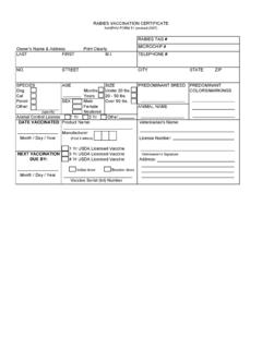
Owner's Name & Address Print Clearly LAST FIRST M.I ...
www.nasphv.orgRABIES VACCINATION CERTIFICATE NASPHV FORM 51 (revised 2007) RABIES TAG # Owner's Name & Address Print Clearly MICROCHIP # LAST FIRST M.I. TELEPHONE #

RC 15 31 - NILIM
www.nilim.go.jp6 生して問題となった損傷が繰り返し載荷される自動車荷重に起因する疲労現象であると考 えられたことから、その対策として行われた部分が多いと考えられるが、一方でこの間に

Inches to mm Conversion - Engineering ToolBox
www.engineeringtoolbox.comInches to mm Conversion Inches Metric Inches Metric Inches Metric Inches Metric Fractional Decimal mm Fractional Decimal mm Fractional Decimal mm Fractional Decimal mm