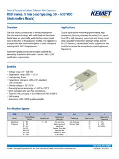
Transcription of Surface Mount - Mounting Pad Dimensions and …
1 1 Surface Mount - Mounting Pad Dimensions and ConsiderationsCeramic Capacitors(including 0603, 0402, 0201and ceramic arrays)Tantalum Capacitors(including low profile andlarge case (X & E) sizesand R case sizes)Aluminum Capacitors(including D, V, & Xcase sizes)by Jim BergenthalF-2100E 6/00 Electronics Corporation P. O. Box 5928 Greenville, SC 29606 Phone (864) 963-6300 Fax (864) 23 The Institute for Interconnnecting and Packaging Electronic Circuits (IPC) hasreleased IPC-SM-782, revision A. Many hours went into this revision.
2 The committeethat developed this document is very large and represents the leaders in many areas ofthe Surface Mount industry. The results are excellent, and we recommend you buy acopy. (The reference section of this bulletin lists the address and phone number forIPC.) This KEMET Bulletin is meant to supplement IPC 782A with focus on ceramic,tantalum and aluminum capacitors. KEMET Surface Mount Aluminum Capacitors areoffered in some of the same case sizes as KEMET Surface Mount Tantalum KEMET catalogs for objectives of this KEMET Bulletin are: To introduce and summarize the methodology used in IPC 782A.
3 To detail the land patterns for wave solder and reflow soldering using themethodology of IPC 782A for ceramic, tantalum and aluminum capacitors. To extend the methodology, and detail land Dimensions for ceramic, tantalumand aluminum capacitor sizes not included in IPC 782A. To detail land patterns for capacitor arrays. To note some errors in IPC 782 and provide corrections. To show the impact of these corrections. To compare the new land patterns (IPC 782A methodology) to thosepreviously presented in KEMET Engineering Bulletin F2100C.
4 To discuss special care needed for small chips, such as 0603, 0402, 0201and for capacitor arrays. To begin discussion of pads for 0201 size ceramic discussion of this Bulletin is certainly in the spirit of IPC 782A. IPC 782 Apresents the equations and methodologies. Having said that, both the IPC and KEMET remind the user that they are responsible for additional modifications as needed thatmay result in a higher level of BASICS: CALCULATIONS AND TOLERANCESI ntroduction:IPC 782A is a very thorough document.
5 We suggest you review the total document,as it has much to offer. The discussions on grids, tolerances, dimension techniques andother aspects are very thorough and helpful in understanding the results. To jumpdirectly to the land patterns and use them blindly is selling the total process short. TheIPC also provides an excellent series of seminars to help you through the present the following synopsis as a baseline understanding. Figure 1 details thedimension letter callouts for pad design. Figure 2 details the equations for calculation ofthe pad Dimensions and critical :Calculation of three pad Dimensions are needed.
6 These are the width (X) of the pad,the overall length (Z) of the pad set, and the separation (G) between pads. The balanceof the Dimensions , including the length of the individual pad (Y), are calculated forreference. The equation that determines the spacing between the pads (G) uses thespacing between the part terminations (Smax), the minimum solder joint desired at theheel or inside joint (JH), and the tolerances at the heel fillet (TH). The equation thatdetermines the overall length of the pads (Z) uses the minimum length of thecomponent (Lmin), the minimum solder joint desired (JT)( this is the one you normallysee), and the tolerances at the toe fillet (TT).
7 The equation that determines the width ofthe pads (X) uses the minimum width (Wmin) of the termination, the minimum sidesolder fillet desired (JS), and the tolerances at the width or side of the termination (TS).4 The IPC calculation for combination of tolerances always uses the square root ofthe sum of the squares method. This is a common engineering practice used when thetolerances vary independent of each other. Calculation of the tolerances about the toeof the part (TT) incorporates the tolerance variation of the length of the part (CL), thetolerance variation of the circuit board artwork and location of tooling holes (F), and thetolerance variations of the placement (P).
8 IPC 782A makes assumptions for F = mmand P = mm. The document also suggests that these should be modified asappropriate by the experience of the user. Calculations of the tolerance variation of thepart are in the dimensional table for each (CL, CW, and CS). The subscripts of C referto the dimension letter callout of the part (L, W, or S). Calculations of total tolerancesuse the square root of the sum of the squares method. For instance, if CL = mm,then TT = ( + + ) = Other combined tolerances use the samecalculation method.
9 For TS the dimensional tolerances of CW are used, and for TH thedimensional tolerances of CS are calculation of S, the spacing between the inside edges of the terminations, isim-portant. The part manufacturers have not usually considered this dimension many cases it is not specified, and must be calculated with the use of termination andlength Dimensions . The standard for tantalum chip capacitors (EIA 535) specifies a min-imum S for all case sizes. The standard for ceramic chip capacitors (EIA 198) specifiesa minimum S for the smallest case variations.
10 This number is key in the calculation of G,one of the main pad dimension calculations. IPC 782A (paragraph ) hasdetermined that the worst-case calculation of Smax would not be representative of thetrue variations. Calculation of Smax also employs the square root of the sum of thesquares method. The tolerances of the length (CL) and the tolerance of the terminationare = Smin + (CL2 + {Tmax - Tmin} 2) = Lmin - 2*Tmax, unless otherwise specified in the part DIMENSIONSF igures 3 and 4 and Tables 1 and 2 detail the Dimensions for ceramic and tantalumchip capacitors.