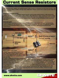
Transcription of SURFACE MOUNT RESISTORS TECHNICAL GUIDE Ver
1 Circuit Components Business Division Automotive & Industrial Systems Company Panasonic Corporation TECHNICAL GUIDE 1 Contents 1. First: 2 page 2. Construction of SURFACE MOUNT RESISTORS : 3 page 3. Manufacturing Method of Thick- film Chip RESISTORS : 4 page 4. System of SURFACE MOUNT RESISTORS : 5 page 5. Kinds of SURFACE MOUNT RESISTORS : 6 page 6. Reliability: 7 page 7.
2 Failure Mechanism: 8 page 8. Application Notes: 9 to 10 page 9. Technique Circuit Design: 11 to 17 page Design of Printed Substrate: 18 to 19 page Used Environment: 20 to 22 page Mounted Method: 22 to 25page 10. TECHNICAL Trend in the Future: 26 to 27 page TECHNICAL GUIDE 21. First Fixed RESISTORS are principal electronic components composed electronic circuit.
3 They are developed with demands of various electronic circuits and used. This TECHNICAL GUIDE is summarized the application technique about SURFACE MOUNT RESISTORS used for electric machine and tools, especially, which need high density MOUNT in these fixed RESISTORS , For selection of various SURFACE MOUNT RESISTORS , confirm with the characteristic of that circuit, in general, following step is proper. (1) Single chip resistor or Composite chip resistor (2) Single chip resistor : Thick- film chip resistor or Thin- film chip resistor (3) Composite chip resistor : Chip resistor array (common terminal circuit) or Chip resistor network (isolated circuit) (4) Select the shape of SURFACE MOUNT RESISTORS in accordance with using voltage (power). In our company, there are numerous kinds of SURFACE MOUNT RESISTORS in order to respond customer s various needs.
4 However, we are happy if you could understand the contents of this TECHNICAL GUIDE , and talk over TECHNICAL contents with us before use, so that you can use it more stability. Moreover, it is separately introduced as for other fixed RESISTORS , components of noise countermeasure and so on. This TECHNICAL GUIDE might change. TECHNICAL GUIDE 32. Construction of SURFACE MOUNT RESISTORS The construction figures of representative SURFACE MOUNT RESISTORS are shown below (Fig 1 to Fig 6). It is different a little by the application of SURFACE MOUNT RESISTORS . Foundation substrate: alumina substrate, Termination: thick- film conductive element, Resistance: thick- film resistor or thin- film resistor . Thick- film chip resistor Thin- film chip resistor Chip resistor array (concave-type) Chip resistor array (convex-type) Chip resistor network (concave-type) Chip resistor network (convex-type) ( ) Thin film (NiCr)Inner terminationMiddle terminationOuter terminationProtective coatingHigh purity ceramic substrateProtective coatingInner termination(thick film )Middle termination (Ni plating)Outer termination(sn plating)
5 Thick- film resistive elementHigh purityalumina substrateThick- film resistive elementProtective coatingThick- film conductive elementHigh purityalumina substrateThick-filmresistive elementProtective coatingThick-filmconductive elemetHigh purityalumina substrateProtective coating Thick- film resistive element Thick- film conductive elementHigh purity alumina substrate Thick- film resistive elementProtective coating(Resin) Inner termination Middle termination (Ni plating) Outer termination (Sn plating) High purity alumina substrate Termination (Thick- film Au) TECHNICAL GUIDE 43. Manufacturing Method of Thick- film Chip RESISTORS Manufacturing method of thick film chip RESISTORS of SURFACE MOUNT RESISTORS (the most representative) is shown Manufacturing process chart of thick- film chip resistor Termination (upper)Termination (back)Breaking slotResistancePre-coat glassTrimming slotProtective coatingSubstrate subjected to first breakingPlating filmSubstrate subjected tosecondary breakingTerminationElectrode formationResistance printingCalcinedPre-coat glass printingCalcinedRevise resistance valueProtective resin printingHardnessFirst breakingSecondary breakingElectrode platingPckaging (taping.)
6 Bulk)ShipmentElectrode spreadHardnessAlumina substrate Electrode paste Resistance paste Glass paste Protective resinpaste Electrode (resin)paste Plating material Packaging material TECHNICAL GUIDE 54. System of SURFACE MOUNT RESISTORS The range of resistance value and resistance temperature characteristic (TCR) of thick- film chip resistor (by kind) are shown in System figure of thick- film chip resistor The range of resistance value and TCR of thin- film chip resistor (by kind) are shown in System figure of thin- film chip resistor The range of resistance value and TCR of thin- film chip resistor (by kind) are shown in System figure of thin- film chip resistor (low resistance value) (1608) (ppm/ C)ERA6Y(2012) (ppm/ C)100m10m300400-300-4001mERJL ERJ12R,14R,1 WRERJ6R, 100ppm 50ppm (ppm/ C)Resistance value (ohm) 101001K10K100K1M10M 600 500 400 300 200 100 0 -100 -200 -300 -400 -500 -600 Resistance temperature characteristic (ppm / degree) general 100ppm type 50ppm type Resistance temperature characteristic (ppm / degree)
7 200 100 0 -100 -200 Resistance temperature characteristic (ppm / degree) 400 100 0 300 -100 -200 -300 200 -400 Resistance value (ohm) 101001K10K100K1M10M ERA3Y (1608)ERA6Y (2012) ERJM1 ERJL ERJ12R, 14R, 1WR ERJ6R, 8R Resistance value (ohm) GUIDE 65. Kinds of SURFACE MOUNT RESISTORS Kinds of SURFACE MOUNT RESISTORS SURFACE MOUNT resistor Single Chip resistor Composite ChipResistor Thick- film ChipResistor Thin- film Chip resistor Chip resistor Array resistor Network General High-precision High-function High-precision High-function Concave termination Convex termination Concave termination Convex termination 5% (J-level) 2% (G-level) 1% (F-level) (D-level) (D-level) (B-level)Anti-serge Anti-sulfurationTrimmable Fuse resistorLow resistancevalue Thermal sensitivechip 2-element 4-element 2-element 4-element 8-element 8-element 8-element 15-element TECHNICAL GUIDE 76. Reliability Field failure rate of SURFACE MOUNT RESISTORS (thick- film chip RESISTORS ) is shown in the table-1.
8 (Set : television) Table-1: Field failure rate Failure rate (fit) Products (Shape) Quantity of used parts (n) Used time (n x T) Failure(r) Point estimation ( 0) Reliability level 60% ( 60) ERJ2G (1005) (From 1990) 1013 (From 1990) 0 ERJ3G (1608) 1010 (From 1986) 1014 (From 1986) 0 ERJ6G (2012) 1011 (From 1986) 1015 (From 1986) 0 ERJ8G (3216) 1010 (From 1986) 1014 (From 1986) 0 ERJ14 (3225) 109 (From 1987) 1012 ( From 1987) 0 ERJ12 (4532) 109 (From 1987) 1012 (From 1987) 0 ERJ1W (6432) 108 (From 1990) 1011 (From 1990) 0 Used time (T) = Use 6 hours / a day 365 days <Calculating method of failure rate> Reliability level = 60% Reliability guaranteed coefficient of market fraction defective X2 {2 (r + 1), } (When it is 0 ) 2 = Market fraction defective 60 = X2 {2 (r + 1), } 109 2 (n X T) = X109 (f i t) n T TECHNICAL GUIDE 87.
9 Failure Mechanism Failure mechanism of thick- film chip resistor and chip resistor array is shown in , Failure mechanism of thin- film chip resistor is shown in As destruction mode, it could be resistance value open or large changing of resistance value, it could not be short circuit mode of RESISTORS , Failure mechanism (Chip fixed RESISTORS , Chip resistor array, Chip resistor network) Failure mode Failure mechanism Manufacturing factor Application factor Oven Electrode crack Solder stressThin electrode- film Ununiform Solder breaking Electrode corrosion Solder degradation resistor chipping Crack Large change of Resistance value Voltage breakdown Voltage degradation Transition of electrode material Temperaturerising Temperaturerising Glass chippingQuantity of solder Unbalance Resin for mold Unsuitable pattern designStress of P-board Unsuitable of soldering condition Sulfur atmosphere Over-load Thin-middle-Ni Ununiform Large of division stressShape defective Inner loss of resistor Large of MOUNT zipper power Large of pulse-load Large of static electricityLot of pulse-times Over-load TECHNICAL GUIDE 9 Failure mechanism of thin- film chip RESISTORS 8.
10 Application Note Precautions in handling RESISTORS Our products are intended for use in general standard applications for general electronic equipment (AV products, household electric appliances, office equipment, information and communication equipment, etc.); hence, they do not take the use under the following special environments into consideration. Accordingly, the use in the following special environments, and such environments, and such environmental conditions may affect the performance of the products; prior to use, verify the performance, reliability, etc. (1). Use in liquids such as water, oil, chemical, and organic solvent. (2). Use under direct sunlight and in outdoor and dusty atmospheres. (3). Use in places full of corrosive gasses such as sea breeze, Cl2, H2O, NH3, SO2, and NOX. (4). Use in environment with large static electricity and strong electromagnetic waves.