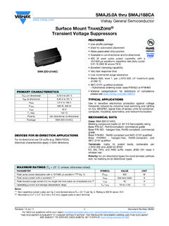
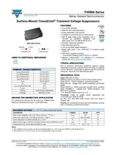
Transcription of Surface-Mount TRANSZORB Transient Voltage Suppressors
1 Thru General Semiconductor Revision: 30-Jun-20211 Document Number: 88392 For technical questions within your region: DOCUMENT IS SUBJECT TO CHANGE WITHOUT NOTICE. THE PRODUCTS DESCRIBED HEREIN AND THIS DOCUMENTARE SUBJECT TO SPECIFIC DISCLAIMERS, SET FORTH AT TRANSZORB Transient Voltage SuppressorsLINKS TO ADDITIONAL RESOURCESDEVICES FOR BIDIRECTION APPLICATIONSFor bidirectional devices use CA suffix ( SMBJ10CA). Electrical characteristics apply in both APPLICATIONSUse in sensitive electronics protection against Voltage transients induced by inductive load switching and lighting on ICs, MOSFET, signal lines of sensor units for consumer, computer, industrial, and Low profile package Ideal for automated placement glass passivated chip junction Available in unidirectional and bidirectional 600 W peak pulse power capability with a 10/1000 s waveform, repetitive rate (duty cycle).
2 % Excellent clamping capability Very fast response time Low incremental surge resistance Meets MSL level 1, per J-STD-020, LF maximum peak of 260 C AEC-Q101 qualified available - Automotive ordering code: base P/NHE3 or P/NHM3 Material categorization: for definitions of compliance please see DATACase: SMB (DO-214AA) Molding compound meets UL 94 V-0 flammability rating Base P/N-E3 - RoHS-compliant, commercial grade Base P/N-M3 - halogen-free, RoHS-compliant, commercial grade Base P/NHE3_X - RoHS-compliant and AEC-Q101 qualified Base P/NHM3_X - halogen-free, RoHS-compliant, and AEC-Q101 qualified ( _X denotes revision code A, B.)
3 Terminals: matte tin plated leads, solderable per J-STD-002 and JESD 22-B102 E3, M3, HE3, and HM3 suffix meets JESD 201 class 2 whisker testPolarity: for unidirectional types the band denotes cathode end, no marking on bidirectional types Notes(1)Non-repetitive current pulse, per fig. 3 and derated above TA = 25 C per fig. 2(2)Mounted on " x " ( mm x mm) copper pads to each terminalPRIMARY CHARACTERISTICSVBR (bidirectional) V to 231 VVBR (unidirectional) V to 231 V to 188 VPPPM600 WIFSM (unidirectional only)100 ATJ CPolarityUnidirectional, bidirectionalPackageSMB (DO-214AA)SMB (DO-214AA)Cathode(unidirectional)(bidire ctional)Anode333 DDD3D3D ModelsAvailableAvailableMAXIMUM RATINGS (TA = 25 C unless otherwise noted)PARAMETER SYMBOL VALUEUNIT Peak pulse power dissipation with a 10/1000 s waveform (1)(2) (fig.)
4 1)PPPM600 W Peak pulse current with a 10/1000 s waveform (1)IPPM See next table A Power dissipation on infinite heatsink at TA = 50 forward surge current ms single half sine-wave unidirectional only (2)IFSM 100A Operating junction and storage temperature rangeTJ, TSTG -55 to +150 C thru General Semiconductor Revision: 30-Jun-20212 Document Number: 88392 For technical questions within your region: DOCUMENT IS SUBJECT TO CHANGE WITHOUT NOTICE.
5 THE PRODUCTS DESCRIBED HEREIN AND THIS DOCUMENTARE SUBJECT TO SPECIFIC DISCLAIMERS, SET FORTH AT (1) Pulse test: tp 50 ms(2) Surge current waveform per fig. 3 and derate per fig. 2(3) For bidirectional types having VWM of 10 V and less, the ID limit is doubled(4) All terms and symbols are consistent with ANSI/IEEE (5) For the bidirectional , the maximum VBR is V(6) VF = V max. at IF = 50 A (unidirectional only)(+) Underwriters laboratory recognition for the classification of protectors (QVGQ2) under the UL standard for safety 497B and file number E136766 for both uni-directional and bi-directional devicesELECTRICAL CHARACTERISTICS (TA = 25 C unless otherwise noted)DEVICE TYPE MODIFIED J BEND LEADDEVICE MARKING CODEBREAKDOWN Voltage VBR AT IT (1) (V) TEST CURRENT IT (mA) STAND-OFF Voltage VWM (V)MAXIMUM REVERSE LEAKAGEAT VWMID ( A) (3)MAXIMUM PEAK PULSE SURGE CURRENTIPPM (A) (2)
6 MAXIMUM CLAMPING Voltage AT IPPM VC (V)MAXIMUM TEMPERATURE COEFFICIENT OF VBR(%/ C) (+) (5) KE KE (+) KG KG (+) KK AK (+) KM KM (+) KP AP (+) KR AR (+) KT AT (+) KV AV (+)SMBJ10A KX AX (+)SMBJ11A KZ KZ (+)SMBJ12A LE BE (+)SMBJ13A LG LG (+)SMBJ14A LK BK (+)SMBJ15A LM BM (+)SMBJ16A LP LM (+)SMBJ17A LR LR (+)SMBJ18A LT BT (+)SMBJ20A LV LV (+)SMBJ22A LX BX (+)SMBJ24A LZ BZ (+)SMBJ26A ME CE (+)SMBJ28A MG MG (+)SMBJ30A MK CK (+)SMBJ33A MM CM (+)
7 SMBJ36A MP CP (+)SMBJ40A MR CR (+)SMBJ43A MT CT (+)SMBJ45A MV MV (+)SMBJ48A MX MX (+)SMBJ51A MZ MZ (+)SMBJ54A NE NE (+)SMBJ58A NG NG (+)SMBJ60A NK NK (+)SMBJ64A NM NM (+)SMBJ70A NP NP (+)SMBJ75A NR NR (+)SMBJ78A NT NT (+)SMBJ85A NV NV (+)SMBJ90A NX NX (+)SMBJ100A NZ NZ (+)SMBJ110A PE PE (+)SMBJ120A PG PG (+)SMBJ130A PK PK (+)SMBJ150A PM PM (+)SMBJ160A PP PP (+)SMBJ170A PR PR PS PS thru General Semiconductor Revision: 30-Jun-20213 Document Number.
8 88392 For technical questions within your region: DOCUMENT IS SUBJECT TO CHANGE WITHOUT NOTICE. THE PRODUCTS DESCRIBED HEREIN AND THIS DOCUMENTARE SUBJECT TO SPECIFIC DISCLAIMERS, SET FORTH AT (1)Mounted on minimum recommended pad layoutNote(1)AEC-Q101 qualifiedTHERMAL CHARACTERISTICS (TA = 25 C unless otherwise noted)PARAMETERSYMBOLVALUEUNITT ypical thermal resistance, junction to ambient (1)R JA 100 C/ WTypical thermal resistance, junction to leadR JL20 ORDERING INFORMATION (Example)PREFERRED P/NUNIT WEIGHT (g)
9 PREFERRED PACKAGE CODEBASE QUANTITYDELIVERY " diameter plastic tape and " diameter plastic tape and (1) " diameter plastic tape and (1) (1) " diameter plastic tape and (1) thru General Semiconductor Revision: 30-Jun-20214 Document Number: 88392 For technical questions within your region: DOCUMENT IS SUBJECT TO CHANGE WITHOUT NOTICE. THE PRODUCTS DESCRIBED HEREIN AND THIS DOCUMENTARE SUBJECT TO SPECIFIC DISCLAIMERS, SET FORTH AT AND CHARACTERISTICS CURVES (TA = 25 C unless otherwise noted)Fig. 1 - Peak Pulse Power Rating CurveFig.
10 2 - Pulse Power or Current vs. Initial junction TemperatureFig. 3 - Pulse WaveformFig. 4 - Typical junction CapacitanceFig. 5 - Typical Transient Thermal ImpedanceFig. 6 - Maximum Non-Repetitive Peak Forward Surge 1 10 100 s s 10 s 100 s ms 10 ms x " ( x mm)Copper Pad AreasPPPM - Peak Pulse Power (kW)td - Pulse Width (s)0 2550751001007550250125150175200TJ - Initial Temperature ( C)Peak Pulse Power (PPP) or Current (IPP)Derating in Percentage, % - Peak Pulse Current, % IRSMt - Time (ms)tr = 10 sPeak ValueIPPMHalf Value -IPPMIPP210/1000 s Waveformas defined by = 25 CPulse Width (td)