Transcription of Virtex-5 FPGA Data Sheet: DC and Switching …
1 DS202 ( ) June 17, Specification1 2006 2010, 2014, 2016 xilinx , Inc. xilinx , the xilinx logo, Artix, ISE, Kintex, Spartan, virtex , Vivado, Zynq, and other designated brands included herein are trademarks of xilinx in the United States and other countries. PowerPC is a trademark of IBM Corp. and is used under license. PCI, PCI Express, PCIe, and PCI-X are trademarks of PCI-SIG. All other trademarks are the property of their respective FPGA Electrical CharacteristicsVirtex -5 fpgas are available in -3, -2, -1 speed grades, with -3 having the highest performance.
2 Virtex-5 FPGA DC and AC characteristics are specified for both commercial and industrial grades. Except the operating temperature range or unless otherwise noted, all the DC and AC electrical parameters are the same for a particular speed grade (that is, the timing characteristics of a -1 speed grade industrial device are the same as for a -1 speed grade commercial device). However, only selected speed grades and/or devices might be available in the industrial supply voltage and junction temperature specifications are representative of worst-case conditions.
3 The parameters included are common to popular designs and typical Virtex-5 FPGA data sheet , part of an overall set of documentation on the Virtex-5 family of fpgas , is available on the xilinx website: Virtex-5 Family Overview Virtex-5 FPGA User Guide Virtex-5 FPGA Configuration Guide Virtex-5 FPGA XtremeDSP Design Considerations Virtex-5 FPGA Packaging and Pinout Specification Embedded Processor Block in Virtex-5 fpgas Reference Guide Virtex-5 FPGA RocketIO GTP Transceiver User Guide Virtex-5 FPGA RocketIO GTX Transceiver User Guide Virtex-5 FPGA Embedded Tri-Mode Ethernet MAC User Guide Virtex-5 FPGA Integrated Endpoint Block User Guide for PCI Express Designs Virtex-5 FPGA System Monitor User Guide Virtex-5
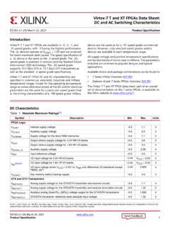
4 FPGA PCB Designer s GuideAll specifications are subject to change without FPGA DC characteristics 0 Virtex-5 FPGA Data Sheet: DC and Switching CharacteristicsDS202 ( ) June 17, 201600 Product SpecificationTable 1:Absolute Maximum RatingsSymbolDescriptionUnitsVCCINTI nternal supply voltage relative to GND to supply voltage relative to GND to drivers supply voltage relative to GND to memory battery backup supply to reference voltage to (3) I/O input voltage relative to GND(4) (user and dedicated I/Os) to I/O input voltage relative to GND (restricted to maximum of 100 user I/Os)(5) to (Commercial Temperature)V to (Industrial Temperature)
5 Or below I/O input voltage relative to GND (user and dedicated I/Os) to VCCO+ applied to an I/O pin, powered or unpowered 100mATotal current applied to all I/O pins, powered or unpowered 100mAVTSV oltage applied to 3-state output(4) (user and dedicated I/Os) to applied to 3-state or below output (user and dedicated I/Os) to VCCO+ temperature (ambient) 65 to 150 CTSOLM aximum soldering temperature(2)+220 CTJM aximum junction temperature(2)+125 CNotes: beyond those listed under Absolute Maximum Ratings might cause permanent damage to the device.
6 These are stress ratings only, and functional operation of the device at these or any other conditions beyond those listed under Operating Conditions is not implied. Exposure to Absolute Maximum Ratings conditions for extended periods of time might affect device soldering guidelines, refer to UG112: Device Package User Guide. For thermal considerations, refer to UG195: Virtex-5 FPGA Packaging and Pinout Specification on the xilinx I/O absolute maximum limit applied to DC and AC signals. I/O operation, refer to UG190: Virtex-5 FPGA User Guide, Chapter 6, I/O Design more flexibility in specific designs, a maximum of 100 user I/Os can be stressed beyond the normal specification for no more than 20% of a data FeedbackVirtex-5 FPGA Data sheet : DC and Switching CharacteristicsDS202 ( ) June 17, Specification2 Table 2.
7 Recommended Operating ConditionsSymbolDescriptionTemperature RangeMinMaxUnitsVCCINTI nternal supply voltage relative to GND, TJ=0 C to +85 supply voltage relative to GND, TJ= 40 C to +100 (1)Auxiliary supply voltage relative to GND, TJ=0 C to +85 supply voltage relative to GND, TJ= 40 C to +100 (2,4,5)Supply voltage relative to GND, TJ=0 C to +85 voltage relative to GND, TJ= 40 C to +100 supply voltage relative to GND, TJ=0 C to +85 CCommercialGND supply voltage relative to GND, TJ= 40 C to +100 CIndustrialGND and below supply voltage relative to GND, TJ=0 C to +85 CCommercialGND VCCO+ and below supply voltage relative to GND, TJ= 40 C to +100 CIndustrialGND VCCO+ (6)
8 Maximum current through any pin in a powered or unpowered bank when forward biasing the clamp diodeCommercial10mAIndustrial10mAVBATT(3 )Battery voltage relative to GND, TJ=0 C to +85 voltage relative to GND, TJ= 40 C to +100 : maximum voltage drop for VCCAUX is 10 data is retained even if VCCO drops to is required only when using bitstream encryption. If battery is not used, connect VBATT to either ground or VCCO of , , , , and configuration supply voltage VCC_CONFIG is also known as total of 100 mA per bank should not be 3.
9 DC characteristics Over Recommended Operating ConditionsSymbolDescriptionData RateMinTypMaxUnitsVDRINTData retention VCCINT voltage (below which configuration data might be lost) retention VCCAUX voltage (below which configuration data might be lost) leakage current per pin10 AILI nput or output leakage current per pin (sample-tested)10 ACINI nput capacitance (sample-tested)8pFIRPU(1)Pad pull-up (when selected) @ VIN=0V, VCCO= APad pull-up (when selected) @ VIN=0V, VCCO= APad pull-up (when selected) @ VIN=0V, VCCO= APad pull-up (when selected) @ VIN=0V, VCCO= APad pull-up (when selected) @ VIN=0V, VCCO= AIRPD(1)Pad pull-down (when selected) @ VIN= 5110 AIBATT(2)Battery supply current150nAnTemperature diode ideality Notes: values are specified at nominal voltage, 25 value specified for worst case process at 25 FeedbackVirtex-5 FPGA Data sheet .
10 DC and Switching CharacteristicsDS202 ( ) June 17, Specification3 Important NoteTypical values for quiescent supply current are now specified at nominal voltage, 85 C junction temperatures (Tj). xilinx recommends analyzing static power consumption at Tj= 85 C because the majority of designs operate near the high end of the commercial temperature range. Data sheets for older products ( , virtex -4 devices) still specify typical quiescent supply current at Tj= 25 C. Quiescent supply current is specified by speed grade for Virtex-5 devices.
