Search results with tag "Switching characteristics"
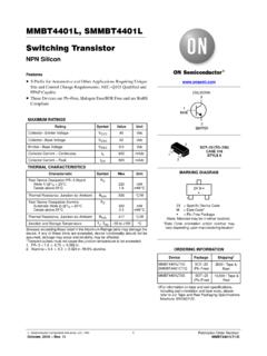
MMBT4401L, SMMBT4401L Switching Transistor
www.onsemi.comSWITCHING CHARACTERISTICS Delay Time (V CC = 30 Vdc, VEB = 2.0 Vdc, IC = 150 mAdc, IB1 = 15 mAdc) td − 15 ns Rise Time tr − 20 Storage Time (V CC = 30 Vdc, IC = 150 mAdc, IB1 = IB2 = 15 mAdc) ts − 225 ns Fall Time tf − 30 Product parametric performance is indicated in the Electrical Characteristics for the listed test conditions, unless ...
Kintex UltraScale FPGAs Data Sheet: DC and AC Switching ...
www.xilinx.comKintex UltraScale FPGAs Data Sheet: DC and AC Switching Characteristics DS892 (v1.19) September 22, 2020 www.xilinx.com Product Specification 2 VBATT Key memory battery backup supply –0.500 2.000 V IDC Available output current at the pad –20 20 mA IRMS Available RMS output current at the pad –20 20 mA GTH and GTY Transceivers
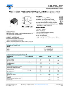
Optocoupler, Phototransistor Output, with Base Connection
www.vishay.comDC current transfer ratio (1) VCE = 10 V, IF = 10 mA 4N35 CTRDC 100 % 4N36 CTRDC 100 % 4N37 CTRDC 100 % VCE = 10 V, IF = 10 mA, TA = - 55 °C to + 100 °C 4N35 CTRDC 40 50 % 4N36 CTRDC 40 50 % 4N37 CTRDC 40 50 % SWITCHING CHARACTERISTICS PARAMETER TEST CONDITION SYMBOL MIN. TYP. MAX. UNIT Switching time (1) VCC = 10 V, IC = 2 …
Virtex-7 T and XT FPGAs Data Sheet: DC and AC Switching ...
www.xilinx.comVirtex-7 T and XT FPGAs Data Sheet: DC and AC Switching Characteristics DS183 (v1.29) March 23, 2021 www.xilinx.com Product Specification 4 IRPU Pad pull-up (when selected) @ VIN =0V V, CCO = 3.3V 90 – 330 µA Pad pull-up (when selected) @ VIN =0V V, CCO = 2.5V 68 – 250 µA Pad pull-up (when selected) @ VIN =0V V, CCO = 1.8V 34 – 220 µA Pad pull-up …
Kintex-7 FPGAs Data Sheet: DC and AC Switching ...
www.xilinx.comKintex-7 FPGAs Data Sheet: DC and AC Switching Characteristics DS182 (v2.16.1) August 7, 2018 www.xilinx.com Product Specification 3 VCCAUX_IO (6) Auxiliary supply voltage when set to 1.8V 1.71 1.80 1…
Xilinx DS152 Virtex-6 FPGA Data Sheet: DC and AC Switching ...
www.xilinx.comVirtex-6 FPGA Data Sheet: DC and Switching Characteristics DS152 (v3.6) March 18, 2014 www.xilinx.com Product Specification 4 Important Note Typical values for quiescent supply current are specified at nominal voltage, 85°C junction temperatures (T j).Xilinx

Artix-7 FPGAs Data Sheet: DC and AC Switching ...
www.xilinx.comArtix-7 FPGAs Data Sheet: DC and AC Switching Characteristics DS181 (v1.25) June 18, 2018 www.xilinx.com Product Specification 2 IDCIN-FLOAT DC input current for receiver input pins DC coupled RX termination = floating – 14 mA IDCIN-MGTAVTT DC input current for receiver input pins DC coupled RX termination = VMGTAVTT – 12 mA IDCIN-GND DC input current for receiver input pins DC …
Virtex-7 T and XT FPGAs Data Sheet: DC and AC …
www.xilinx.comVirtex-7 T and XT FPGAs Data Sheet: DC and AC Switching Characteristics DS183 (v1.27) April 6, 2017 www.xilinx.com Product Specification