Transcription of Vivado Tutorial - Xilinx
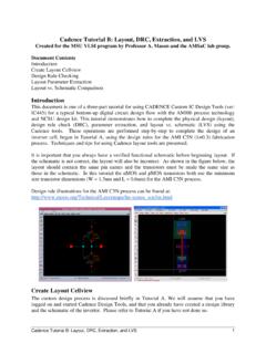
1 Lab Workbook Vivado Tutorial Artix-7 Vivado Tutorial -1 copyright 2015 Xilinx Vivado Tutorial Introduction This Tutorial guides you through the design flow using Xilinx Vivado software to create a simple digital circuit using VHDL. A typical design flow consists of creating model(s), creating user constraint file(s), creating a Vivado project, importing the created models, assigning created constraint file(s), optionally running behavioral simulation, synthesizing the design, implementing the design, generating the bitstream, and finally verifying the functionality in the hardware by downloading the generated bitstream file.
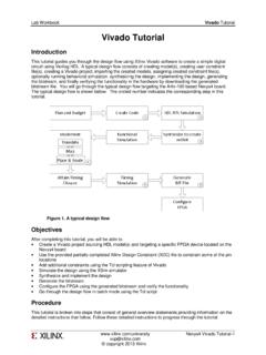
2 You will go through the typical design flow targeting the Artix-7 based Basys3 and Nexys4 DDR boards. The typical design flow is shown below. The circled number indicates the corresponding step in this Tutorial . Figure 1. A typical design flow Objectives After completing this Tutorial , you will be able to: Create a Vivado project sourcing HDL model(s) and targeting a specific FPGA device located on the Basys3 or Nexys4 DDR boards Use the provided user constraint file (XDC) to constrain pin locations Simulate the design using the XSIM simulator Synthesize and implement the design Generate the bitstream Download the design and verify the functionality Procedure This Tutorial is broken into steps that consist of general overview statements providing information on detailed instructions that follow.
3 Follow these detailed instructions to progress through the Tutorial . Vivado Tutorial Lab Workbook Artix-7 Vivado Tutorial -2 copyright 2015 Xilinx Design Description The design consists of some inputs directly connected to the corresponding output LEDs. Other inputs are logically operated on before the results are output on the remaining LEDs as shown in Figure 2. Figure 2. Completed Design General Flow for this Tutorial Create a Vivado project and analyze source files Simulate the design using XSIM simulator Synthesize the design Implement the design Perform the timing simulation Verify the functionality in hardware using Basys3 or Nexys4 DDR board Lab Workbook Vivado Tutorial Artix-7 Vivado Tutorial -3 copyright 2015 Xilinx Create a Vivado Project Step 1 1-1.
4 Launch Vivado and create a project targeting the xc7a35tcpg236-1 (Basys3) or xc7a100tcsg324-1 (Nexys4 DDR) device and using the VHDL. Use the provided and or files from the sources/ Tutorial directory. 1-1-1. Open Vivado by selecting Start > All Programs > Xilinx Design Tools > Vivado > Vivado 1-1-2. Click Create New Project to start the wizard. You will see Create A New Vivado Project dialog box. Click Next. 1-1-3. Click the Browse button of the Project location field of the New Project form, browse to c:\xup\digital, and click Select. 1-1-4. Enter Tutorial in the Project name field.
5 Make sure that the Create Project Subdirectory box is checked. Click Next. Figure 3. Project Name and Location entry 1-1-5. Select RTL Project option in the Project Type form, and click Next. 1-1-6. Select VHDL as the Target Language and as the Simulator language in the Add Sources form. 1-1-7. Click on the Green Plus button, then click on the Add button, browse to the c:\xup\digital\sources\ Tutorial directory, select , click Open, and verify the Copy constraints files into projects box is check. Then click Next. 1-1-8. Click Next at the Add Existing IP form.
6 Vivado Tutorial Lab Workbook Artix-7 Vivado Tutorial -4 copyright 2015 Xilinx 1-1-9. In the Add Constraints form, click on the Green Plus button, then the Add button, browse to the c:\xup\digital\sources\ Tutorial directory, select (for Basys3) or (for Nexys4 DDR), click Open, and then click Next. The XDC constraint file assigns the physical IO locations on FPGA to the switches and LEDs located on the board. This information can be obtained either through a board s schematic or board s user guide. 1-1-10. In the Default Part form, using the Parts option and various drop-down fields of the Filter section, select the xc7a35tcpg236-1 part (for Basy3) or xc7a100tcsg324-1 part (for Nexys4 DDR).
7 Click Next. Figure 4. Part Selection for Basys3 Figure 4. Part Selection for Nexys4 DDR Lab Workbook Vivado Tutorial Artix-7 Vivado Tutorial -5 copyright 2015 Xilinx 1-1-11. Click Finish to create the Vivado project. 1-1-12. Use the Windows Explorer and look at the c:\xup\digital\ Tutorial directory. You will find that the and other directories, and the ( Vivado ) project file have been created. Two sub-directories, constrs_1 and sources_1, are created under the directory; deep down under them, the copied or (constraint) and (source) files respectively are placed.
8 Figure 5. Generated directory structure 1-2. Open the source and analyze the content. 1-2-1. In the Sources pane, double-click the entry to open the file in text mode. The design takes input from slide switches 0 to 7 of the board and toggles the LEDs on the board. Since combinatorial logic is inserted between some switches, the LEDs will turn on/off depending on the pattern of the switches. This is a very basic combinatorial logic demo. Figure 6. Opening the source file 1-3. Open the or source, analyze the content and edit the file. 1-3-1. In the Sources pane, expand the Constraints folder and double-click the (Basys3) or (Nexys4 DDR) entry to open the file in text mode.
9 Vivado Tutorial Lab Workbook Artix-7 Vivado Tutorial -6 copyright 2015 Xilinx Figure 7. Opening the constraint file 1-3-2. Uncomment SW[7:0] by deleting the # sign or by highlighting SW[7:0] and pressing CTRL /. Uncomment LED[7:0]. The pin names will have to be changed to match the pin names in the file. Figure 8. Editing the Basys3 Master XDC Figure 8. Editing the Nexys4 DDR Master XDC Lab Workbook Vivado Tutorial Artix-7 Vivado Tutorial -7 copyright 2015 Xilinx 1-3-3. Change the sw[*] name to swt[*], and LED[*] to led[*] as the port names in the model are swt and led.
10 1-3-4. Close the or the file saving the changes. 1-4. Perform RTL analysis on the source file. 1-4-1. In the Sources pane, select the entry, and click on Schematic (you may have to expand the Open Elaborated Design entry) under the RTL Analysis tasks of the Flow Navigator pane. A logic view of the design is displayed. Figure 9. A logic view of the design Notice that some of the switch inputs go through gates before being output to LEDs and the rest go straight through to LEDs as modeled in the file. 1-5. I/O constraints 1-5-1. Once RTL analysis is performed, another standard layout called the I/O Planning layout is available.