Transcription of Wet-chemical etching of silicon and SiO2
1 Basics of Microstructuring 01 Chapter MicroChemicals Fundamentals of Microstructuring Wet-chemical etching OF silicon AND SIO 2. silicon is the most common substrate material used in microelectronics and micro-mechanics. It is used not only as a passive substrate, but also as an active material in electronic or mechanical components. The neces- sary patterning can also be achieved by means of Wet-chemical etching methods, as described in this chapter. Anisotropic etching of silicon etching Mechanism Strongly aqueous alkaline media such as KOH-, NaOH- or TMAH-solutions etch crystalline silicon via Si + 2 OH- + 2 H2O Si(OH)4 + H2 SiO2(OH)22- + 2 H2. Because the Si atoms of the di erent crystal planes have di erent activation energies for the etching reaction and the KOH etching of Si is not di usion-limited but etching -rate-limited, the etching process takes place anisotropically: The {100} and {110} planes are much more rapidly etched than the stable {111} plane that act as etch stops.
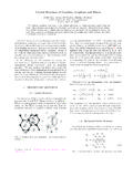
2 (111)-oriented Wafers (111)-oriented Si wafers are hardly attacked by alkaline solutions, since here the entire wafer surface forms an etch stop. Because the real orientation of wafers is usually tilted to a few against the ideal crystal plane, with nominally (111)-oriented wafers, an etching attack in the form of very shallow steps also occurs. (100)-oriented Wafers (100)-orientated wafers in alkaline etchants form square-based pyramids with {111} surfaces. These pyr- amids can be realised on mono-crystalline silicon solar cells for the purpose of re ection minimisation. (110)-oriented Wafers (110)-orientated wafers in alkaline etchants form perpendicular trenches with {111} side-walls, used as micro-channels in micro-mechanics and micro- uidics. Etch Rates The anisotropy, the absolute etch rates and the homogeneity of the etching depend on both defects in Fig. 119: The concentration and temperature-dependent etching rate of (100) and (110) planes of crystalline silicon in KOH.
3 (left graph) and TMAH (right graph). The alkaline etching of Si requires in addition to OH- ions, free water molecules. Therefore, the etching rate, but also the surface roughness of the etched silicon surface, decreases to stronger alkaline solutions. Basics of Microstructuring 01 Chapter MicroChemicals Fundamentals of Microstructuring Fig. 120: The concentration and temperature-dependent selectivity of the etching rate of (100) - Si and SiO2 in TMAH (left graph) and KOH (right graph). In TMAH, the etch rates of Si and SiO2 have their maximum at di erent TMAH concentra- tions, which is why their ratio shows a local minimum. the silicon as well as contamination of the etching by metal ions and already etched Si ions in addition to etching temperature. Also the doping of Si plays an important role: During etching , boron-doped Si forms bo- rosilicate glass on the surface which acts as etch stop if the boron doping concentration exceeds (> 1019 cm-3).
4 Fig. 120 and Fig. 121 show the tempera- ture and concentration-dependent etch rates of (100)- and (110) planes in KOH- and TMAH-solutions (Fig. 119), as well as the se- lectivity of the SiO2 etching (Fig. 120 and Fig. 121), which is often used as masking. Typical etching Mixtures Fig. 121: The ratio of the etching rates of silicon in (100) to the (111) We supply 25% TMAH and 44% KOH in VLSI. direction in TMAH- (orange circular areas) and KOH-solutions (blue- quality. Because these media only attack green) as a function of the respective concentration and tempera- SiO2 to a very small extent, the (native) SiO2. ture lm must be removed before the aniso- tropic Si etching in diluted or bu ered hy- dro uoric acid. Suitable etching Masks The high pH values and temperatures required for the anisotropic etching of silicon attack even heavily cross-linked negative resists in a short time, so that photoresist masks do not come into question for this purpose.
5 Instead, hard masks usually made of silicon nitride, SiO2 or alkaline-stable metal lms such as chromium are used, which in turn can be structured using photoresist masks. Basics of Microstructuring 01 Chapter MicroChemicals Fundamentals of Microstructuring Isotropic etching of silicon with HF/HNO3. etching Mechanism The basic etching mechanism in the isotropic etching of Si is divided into the oxidation of silicon using nitric acid and the etching of the oxide constantly formed on the surface from this with hydro uoric acid: (1) Formation of NO2 from nitric acid: 4 HNO3 4 NO2 + 2 H2O + O2. (2) Oxidation of silicon by NO2: 2 NO2 + Si SiO2 + 2 NO. (3) etching of SiO2: SiO2 + 6 HF H2 SiF6 + 2 H2O. with the formula of the overall reaction: 4 HNO3 + 2 Si + 12 HF . 4 NO + 6 H2O + O2 + 2 H2 SiF6. The resulting hexa uorosilicic acid (H2 SiF6) is stable in aqueous solution. etching Rates of silicon Fig. 122 shows the rate of etching of crystal- line silicon in di erent HF : HNO3 mixtures at room temperature.
6 The etch rate drops towards zero when either the HF or HNO3 concentration be- 100. comes very low, since in pure HF no SiO2. forms which can be etched in HF, and HNO3. 10. only oxidises the Si without etching it. An accurate control of the etching rate requires temperature accuracy within . C. A dilution with acetic acid improves [HNO3 (70%)]. the wetting of the hydrophobic Si-surface and thus increases the spatial homogeneity of the etch rate. Fig. 122: The etching rate of silicon as a function of the HNO3 and HF. Doped (n- and p-type) silicon exhibits a concentration of the etching mixture at room temperature. higher etching rate than undoped silicon . Etch Selectivity of Si : SiO 2 [HF] Tempera- As the etching triangle in Fig. 123 shows, high HF : HNO3 ture depend- ratios promote rate-limited etching (strong temperature ence of the dependency of the etch rate) of Si via the oxidation step. etching rate increases Low HF : HNO3 ratios promote di usion-limited etching (lower temperature dependency of the etch rate).
7 Pure Selec- HF does not attack silicon , pure HNO3 only results in an tivity to oxidation of its surface. SiO2 in- The SiO2 etch rate is determined by the HF-concentra- creases tion, since the oxidation does not play a role. etching of SiO2 with HF or BHF. Hydro uoric Acid [H 2O] (+ [CH3 COOH]) [HNO3]. Hydro uoric acid (HF) is the only Wet-chemical medium with which SiO2 can be isotropically etched at a reasona- Fig. 123: The etching triangle for silicon shows the ble rate. Due to the high toxicity of concentrated HF, one principal dependence of the etching rate on the composition of the etchant. has to consider the concentration that is really required for each individual application. 1 % HF is su cient for re- Basics of Microstructuring 01 Chapter MicroChemicals Fundamentals of Microstructuring moving native SiO2 in a so-called HF-Dip, and even 200 - 300 nm oxide can be etched in 10 % HF or bu - ered HF in a reasonable amount of time.
8 We supply 1 %, 10 % and 50 % HF in VLSI-quality. Bu ered Hydro uoric Acid The etching of Si and SiO2 consumes F-ions via the reaction SiO2 + 4 HF SiF4 + 2 H2O. HF bu ered with ammonia uoride (BHF = NH4F + H2O + HF) : maintains the free F- ion concentration via NH4F + H2O H3O+ + F- + NH3 allowing a constant and controllable etch rate as well as spatial homogeneous etching , an increase in the etch rate (factor - ) by highly reactive HF2- ions and an increase in the pH-value ( minor resist underetching and resist lifting). Despite the increased reactivity, strongly bu ered hydro uoric acid has a pH-value of close to 7 and therefore may not be detected by chemical indicators, We o er bu ered HF (BOE 7: 1 = AF ). in L containers in VLSI quality optionally with or without surfactant for improved wetting and etching homogeneity. Etch Rates of SiO2 in HF or BHF. Compared to thermal oxide, deposited ( CVD) SiO2 has a higher etch rate due to its porosity; wet oxide a slightly higher etch rate than dry (thermal) oxide for the same reason, thermally via O2 produced SiO2.
9 Phosphorus-doped SiO2 etches faster than undoped SiO2. etching of Glasses Unlike SiO2, glasses with various compositions show a strong dependency between their etch rate and additives in the etch. Such additives ( HCl, HNO3) dissolve surface lms formed on the glass during etching , which are often chemically inert in HF and would stop or decelerate glass etching with pure HF. Therefore, such additives allow a continued etching at a constant and high rate. This allows one to in- crease the etch rate at a reduced HF-concentration (= increased stability against resist peeling). Our Photoresists: Application Areas and Compatibilities Resist Film Recommended Re- In general, almost all resists can be used for almost any application. However, the special properties of each resist family Recommended Applications 1 Recommended Developers 3. Resist film thickness achievable and processable with standard equipment under standard conditions. Some resists can Resist Family Photoresists movers 4.
10 Thickness 2. Metal ion free (MIF) developers are significantly more expensive, and reasonable if metal ion free development is re- AZ 1505 m AZ 1512 HS - m be diluted for lower film thicknesses; with additional effort also thicker resist films can be achieved and processed.. AZ 1500 AZ 351B, AZ 326 MIF, AZ 726 MIF, AZ Developer AZ 1514 H - m Also depends on the resist processing and subsrrate materials used, details see section removers' next page AZ 1518 - m AZ 4533 3 - 5 m Improved adhesion for wet etching , no AZ 4500 AZ 400K, AZ 326 MIF, AZ 726 MIF, AZ 826 MIF. AZ 4562 5 - 10 m focus on steep resist sidewalls AZ P4110 1 - 2 m AZ P4330 3 - 5 m AZ P4000 AZ 400K, AZ 326 MIF, AZ 726 MIF, AZ 826 MIF. AZ P4620 6 - 20 m Positive AZ P4903 10 - 30 m AZ 100 Remover, TechniStrip P1316. AZ PL 177 AZ PL 177 3 - 8 m AZ 351B, AZ 400K, AZ 326 MIF, AZ 726 MIF, AZ 826 MIF. TechniStrip P1331. Spray coating AZ 4999 1 - 15 m AZ 400K, AZ 326 MIF, AZ 726 MIF, AZ 826 MIF.