Search results with tag "Etching"

CHAPTER 6: Etching - City University of Hong Kong
www.cityu.edu.hkCHAPTER 6: Etching Different etching processes are selected depending upon the particular material to be removed. As shown in Figure 6.1, wet chemical processes result in isotropic etching where both the vertical and lateral etch rates are comparable, whereas dry etching processes like sputter etching, plasma etching, ion beam etching, and

PLASMA RIE ETCHING FUNDAMENTALS AND ...
www.purdue.eduFUNDAMENTALS AND APPLICATIONSFUNDAMENTALS AND APPLICATIONS 1. O tli 1 Introductory Concepts Outline ... ¾Only used for sputtering system not for etchingOnly used for sputtering system not for etching. Vc=0 Vc= -100 n V( ) X Red: n i Black: n ... The Etching of Si and its Compounds The Etching of Si and its Compounds 6. The Etching of Other ...

VLSI FABRICATION TECHNOLOGY - Oxford University Press
global.oup.comA.1.4 Etching To permanently imprint the photographic patterns onto the wafer, chemical (wet) etching or RIE dry etching procedures can be used. Chemical etching is usually referred to as wet etching. Different chemical solutions can be used to remove different layers. For example, hydrofluoric (HF) acid can be used to etch SiO 2
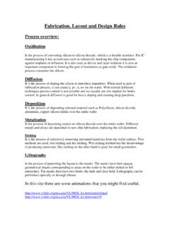
Fabrication, Layout and Design Rules
users.encs.concordia.caEtching It is the process of selectively removing unwanted materials from the wafer surface. Two methods are used, wet etching and dry etching. Wet etching method has the disadvantage of producing undercuts. Dry etching on the other hand is good for small geometries. Lithography Is the process of patterning the layout to the masks.

BOE / HF – Silicon dioxide Etching Standard Operating ...
d1rkab7tlqy5f1.cloudfront.netJul 19, 2018 · BOE / HF – Silicon dioxide Etching Standard Operating Procedure Prepared by: Pauline Stevic Date: July 19, 2018 1. Purpose and application Buffered Oxide Etch (BOE) or just hydrofluoric acid is used for etching silicon dioxide on silicon wafers. Buffered oxide etch is a mixture of hydrofluoric acid and ammonium fluoride.

WET-CHEMICAL ETCHING OF METALS
www.microchemicals.comThe chromium nitrate, which during the etching process forms a dark, constantly new formation on the chromium layer, is very soluble in water and thus in the chromate etchants. Compatibility and Selectivity All of our photoresists are suffi ciently stable in ceric ammonium nitrate and perchloric acid-based etching

1. ETCHING - btu.edu.tr
depo.btu.edu.trElectrolytic etching The electrolytic etching of a sample is done in an electrolysis cell. This process is particularly used for the electrolytic polishing of stainless steel. The solution used in electrolytic polishing may be acidic/basic or salt contained. The samples will be …

CMOS Technology and Logic Gates - MIT OpenCourseWare
ocw.mit.eduWet Etching ETCHING Isotropic Anisotropic UV Light Photomask SiO SiO SiO SiO Photoresist SiO Dry Etching 6.884 – Spring 2005 Figure by MIT OCW. 2/07/2005 L03 – CMOS Technology 9 . FET = Field-Effect Transistor The four terminals of a fet (gate, source, drain and bulk)
Quality Matters PACE Technologies Newsletter …
www.metallographic.comby Donald Zipperian, Ph.D. September 2003 PACE Technologies Etching - Enhancing Microstructures Etching Basics Considerations for chemical etching

Wet Chemical Etching - Basics
microchemicals.comThe stable bonding of the etched atoms to a chemical complex which is suffi ciently soluble in the etching mixture enables a constantly high etching rate. A complex is a structure in which a central atom (usually a metal ion = the etched element) having gaps in its electron confi guration is surrounded by one or more

Recent Advances in GaN Dry Etching Process Capabilities
www.plasma-therm.comAdvances in GaN Dry Etching Process Capabilities Mike DeVre, Applications Lab Manager, Compound Semi & Microtechnology, Unaxis Wafer Processing
Effects of hydrogen on plasma etching for silicon and ...
www.ispc-conference.org21st International Symposium on Plasma Chemistry (ISPC 21) Sunday 4 August – Friday 9 August 2013 Cairns Convention Centre, Queensland, Australia Effects of hydrogen on plasma etching for silicon and silicon nitride

Electro-Etching Workshop
bijoux-de-terre.comJohn Fetvedt www.bijoux-de-terre.com September 14, 2018 7 Electro-Etching 101 Introduction I want to point out that I generally work on one or two small, 1 to 6 inch projects of silver, copper or

CRYSTALLOGRAPHY OF SILICON - MicroChemicals
www.microchemicals.comhigh resolution for e. g. dry etching AZ® 701 MiR AZ® 701 MiR (14 cPs) AZ® 701 MiR (29 cPs) ≈ 0.8 µm ≈ 2 - 3 µm AZ® 351B, AZ® 326 MIF, AZ® 726 MIF, AZ® Developer Posi t iv e ® (ch em. ® amp li fied) Steep r si t sid walls, high r solution and aspect ratio for e. g. dry etching or plating AZ® XT AZ® 12 XT-20PL-05 AZ 12 XT-20PL ...

Introduction to Plasma Etching - University of Texas at Austin
willson.cm.utexas.eduMany of the plasmas used in dry etching are weakly ionized Ionization fraction, x i << 1 Quasineutral: n i = n e densities (~109 –1012 cm-3); magnitudes lower than the neutral gas density (n g) Plasma generated inside etch tool by feeding electrical power into a gas Power transferred to the few free

chromium etching - MicroChemicals
www.microchemicals.euChromium Etching Revised: 2013-11-07 Source: www.microchemicals.com/downloads/application_notes.html Photoresists, wafers, plating solutions, etchants and solvents ...

AN900 APPLICATION NOTE - STMicroelectronics
www.st.comby Microcontroller Division Applications ... Etching process is used to etch into a specific layer the circuit pattern that has been defined during the photomasking process. Etching process usually occurs after deposition of the layer ... system. Any scratch would alter its behaviour (or impact its reliability), any shock would cause
Plasma Etching System and its Applications to 45–32-nm ...
www.hitachi.comPlasma Etching System and its Applications to 45–32-nm Leading-edge Devices 58 accomplished by applying coaxially installed turbo molecular pumps, symmetrically designed electrodes,

Reduction of Device Damage During Dry Etching of …
www.plasmatherm.comReduction of Device Damage During Dry Etching of Advanced MMIC Devices Using Optical Emission Spectroscopy D. Johnson, R. Westerman, M. DeVre, Y. Lee, J. Sasserath
Wet-chemical etching of silicon and SiO2
www.microchemicals.comchromium are used, which in turn can be structured using photoresist masks. Fig. 120: The concentration and temperature-dependent selectivity of the etching rate of (100) - Si and SiO 2

Preparing Concrete Floors For painting
www.resene.co.nzPreparing Concrete Floors for Painting (2004) Acid etching Concrete is alkaline, therefore it can be cleaned and etched with acid. For the acid to work
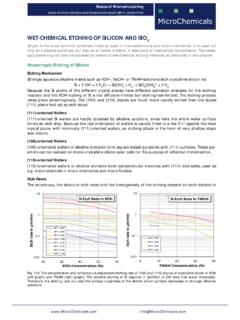
Single Pack High Build Etching Universal Primer - PPG LIC
www.ppglic.com.auData Sheet: 783 Superseded 03/05 Revised 03/08 Composition AMERETCH 783 is a single pack Polyvinyl Butyral based, etch primer containing anti-corrosive

Positive Tone Photosensitive Polyimide Coatings
www.toray.co.jp4 Semiconductor Process photoresist Al passivation Si Photoresist coating Photoresist developing Passivation dry-etching Photoresist stripping PI coating

Novel Polymeric Protective Coatings for Hydrofluoric Acid ...
www.brewerscience.com70nm) was applied, intact films were obtained after HF wet etching, and no oxide loss was observed by prism coupler measurement. Similar results were also obtained when the …
Experiment 3 Metallographic Observations
www.csun.eduother defects can be observed in this way, and if they are identified before etching, subsequent confusion and misinterpretation can be largely avoided. The specimen to …
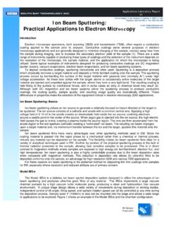
Ion Beam Sputtering: Practical Applications to Electron ...
www.southbaytech.com2 EM Sample Preparation Applications Laboratory Report 91 Figure 1: The Model IBS/e Ion Beam Sputter Deposition and Etching System.The inside of the vacuum chamber is shown at right with the Large Area Stage (LAS) installed.
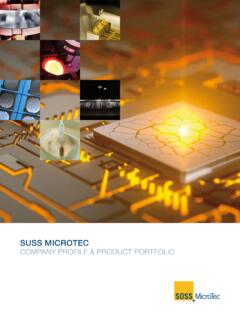
SHAPING THE FUTURE
res.cloudinary.comWith its global infrastruc-ture for applications and service SUSS MicroTec supports more than 8,000 installed systems worldwide. LITHOGRAPHY SYSTEMS ... + Etching MaskTrack Pro/X Automated system 193i 2x / 1x, EUVL and NIL + EUV und 193i Photomask Cleaning + EUV Photomask Automation
AP-42, CH 12.20: Electroplating
www3.epa.govChromium plating and anodizing operations include hard chromium electroplating of metals, ... soak, desmutting, etching, and vapor degreasing. The pretreatment steps used for a particular aluminum substrate depend upon the amount of smut and the composition of the aluminum. The

Surface Treatment of Metals and Plastics
eippcb.jrc.ec.europa.eulocally important are NOX, HCl, HF and acid particulates from pickling operations, hexavalent chromium mist released from hexavalent chromium plating, and ammonia from copper etching in PCB manufacture and electroless plating. Dust, as a combination of abrasives and abraded substrate, is generated by the mechanical preparation of components.

MANUAL FOR SURFACE TREATMENT OF STAINLESS …
www.voestalpine.comOverpickling is a too strong etching of a surface with pick - ling acids. This leaves a rough surface that may result in a lowering of the metal’s properties. NO x is toxic nitric fumes (NO and NO 2) formed during the pickling process. Passivation is the name applied to a number of different processes related to stainless steel. Unless ...

A review of polymer dissolution - University at Buffalo
wwwcourses.sens.buffalo.edunature, aqueous-base developability, and etching resistance, novolak dissolution has become an important process in these applications. Another example where polymer dissolution becomes important is in membrane science, specifi-cally for a technique, called phase inversion, to form asymmetric membranes. In this process, a polymer
Aluminum Electrolytic Capacitors - TDK Electronics AG
www.tdk-electronics.tdk.comSince the electrolytic capacitors have a liquid as a cathode, they are also designated as "wet" or "non-solid" capacitors. The liquid has the advantage that it fills the fine etching pits, therefore opti-mally fitting into the anode structure. The two aluminum foils are separated by paper spacers. The paper serves various purposes, it

CUSTOMER SPEC REVISION TITLE Rolls Royce CME 5033/Sect …
www.paradigmprecision.comApr 02, 2019 · Rolls Royce MSRR 9507-2 6 Chromium Carbide/Nichrome (75/25) Physical Mix Powder Rolls Royce MSRR 9507-304 3 Tungsten Carbide/Cobalt Coating ... Rolls Royce RPS 147 14 Etching Of Hardened Steel Components Rolls Royce RPS 184 28 Fusion Welding Rolls Royce RPS 194 19 Furnace Brazing

Laboratory Exhaust Systems - Greenheck-USA
content.greenheck.comThe Vektor®-H is a cost-effective, self-contained, ... primer, is applied. • Step 3: The finish coat of polyester resin (Hi-Pro Polyester), a super durable class of ... 2 - Surface etching, severe staining, but film integrity remains 3 - Significant pitting, cratering, swelling, or …
Chapter 1.10 - Miscellaneous Etchants
nanolab.berkeley.eduFor VLSI aluminum etching, there is available a pre-mixed phosphoric/acetic acid mixture. ... Etch rate ~ 2000 Å/min. 16 parts phosphoric acid . 2 parts DI water . 1 part acetic acid . 1 part nitric acid . Aluminum Etchants - Others These will not etch gold, etc. Phosphoric acid at 60ºC ... 1 part conc. HF or 50 g CrO: 3: in 100 ml H: 2: O ...
ARDEX FEATHER FINISH
www.ardexamericas.comSelf-Drying, Cement-Based Finish Underlayment Self-drying, finishing underlayment ... not install ARDEX FEATHER FINISH before the primer has dried thoroughly. GYPSUM: If the substrate is a gypsum underlayment that will ... acid etching, adhesive removers, solvents and sweeping compounds are not acceptable means

RODUCT NO 1249-50, 51 - QUIKRETE
www.quikrete.comSelf-Leveling Floor Resurfacer (No. 1249-51) produce a smooth surface ... Acid etching, solvents, and sanding are not acceptable means for preparing the substrate. If installing over wood floors, reinforce to prevent flexing of the floor. Seal all perimeter openings to retain leakage. ...
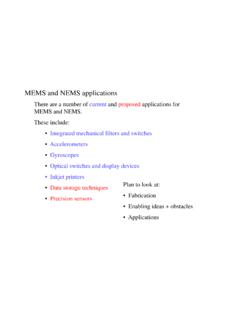
MEMS and NEMS applications - Rice University
www.owlnet.rice.edu• “Wet” etches - HF to remove SiO. 2, KOH to etch Si in preferred directions. Quick, easy, but no directionality - need etch-stops. Surface tension issues! • Reactive Ion Etching (RIE), Inductively Coupled Plasma (ICP)-RIE Highly directional, chemically selective, can be slow. Vertical sidewalls, little or no undercut. Oxford Plasma Tech.

ArmorSeal ARMORSEAL 8100 Heavy WATER BASED EPOXY …
spectrumpainting.compockets and other voids with Steel-Seam FT910. Primer required. Follow the standard methods listed below when applicable: ASTM D4258 Standard Practice for Cleaning Concrete. ASTM D4259 Standard Practice for Abrading Concrete. ASTM D4260 Standard Practice for Etching Concrete. ASTM F1869 Standard Test Method for Measuring Moisture Vapor
Technology Trends and Future History of Semiconductor ...
www.hitachi-chem.co.jp25 Hitachi Chemical Technical Report No.55 PWB was mainly developed in the United States during the 1950s. The etched foil method featuring chemical etching of copper foil on the substrate to formulate a circuit was mainly used for manufacturing PWB.
Similar queries
Etching, Applications, System, And its, VLSI FABRICATION TECHNOLOGY, Oxford University Press, Wet) etching, Wet etching, Chromium, Electrolytic etching, Electrolytic, CMOS, MIT OpenCourseWare, Wet Etching ETCHING, Quality Matters PACE Technologies Newsletter, Basics, Bonding, Dry Etching, Effects of hydrogen on plasma etching, Plasma, Electro-Etching Workshop, Chromium Etching, Plasma Etching System and its Applications, Plasma Etching System and its Applications to 45–32-nm Leading, Reduction of Device Damage During Dry Etching, Devices Using Optical Emission Spectroscopy, Preparing Concrete Floors for Painting, Acid etching Concrete, Acid, Single pack, Polymeric Protective Coatings for Hydrofluoric Acid, Experiment 3 Metallographic Observations, Ion Beam Sputtering: Practical Applications to Electron, Ion Beam, Electroplating, Chromium electroplating, Surface Treatment, Pickling, FOR SURFACE TREATMENT OF STAINLESS, A review of polymer dissolution, Laboratory Exhaust, Self, Primer, Etch, 1 part, 1 part nitric acid, QUIKRETE, MEMS and NEMS applications, Technology Trends and Future History of Semiconductor, Technical