Example: quiz answers
CRYSTALLOGRAPHY OF SILICON - MicroChemicals
high resolution for e. g. dry etching AZ® 701 MiR AZ® 701 MiR (14 cPs) AZ® 701 MiR (29 cPs) ≈ 0.8 µm ≈ 2 - 3 µm AZ® 351B, AZ® 326 MIF, AZ® 726 MIF, AZ® Developer Posi t iv e ® (ch em. ® amp li fied) Steep r si t sid walls, high r solution and aspect ratio for e. g. dry etching or plating AZ® XT AZ® 12 XT-20PL-05 AZ 12 XT-20PL ...
Tags:
Information
Domain:
Source:
Link to this page:
Documents from same domain
Wet-chemical etching of silicon and SiO2
www.microchemicals.comchromium are used, which in turn can be structured using photoresist masks. Fig. 120: The concentration and temperature-dependent selectivity of the etching rate of (100) - Si and SiO 2
Technical Data Sheet Technisches Datenblatt
www.microchemicals.comTechnical Data Sheet Technisches Datenblatt. Development . Immersion Immerse for approximately 60 seconds in either high-contrast or high-speed AZ Developer
Technical Data Sheet Technisches Datenblatt
www.microchemicals.comTechnical Data Sheet Technisches Datenblatt. HANDLING ADVISES . Consult the Material Safety Data Sheets provided by us or your local agent!. This AZ Photoresists are made up with our patented safer solvent PGMEA.

AZ nLOF 20xx Negative Resist - MicroChemicals
www.microchemicals.comMicroChemicals GmbH Ulm – www.microchemicals.com - [email protected] AZ ®® nLOF 20xx Negative Resist ... complement Information for Processing revised 2005-11 …

General Purpose Developer - MicroChemicals
www.microchemicals.comDescription AZ 351B Developer is a general purpose developer for use with almost any positive AZ Photoresist. It was designed to achieve utmost contrast and best wall profile.

Post Exposure Bake (PEB) - microchemicals.com
www.microchemicals.comAZ® 726 MIF is 2.38 % TMAH- (TetraMethylAmmoniumHydroxide) in water, with additional surfactants for rapid and uniform wetting of the substrate (e. g. for puddle development) AZ® 826 MIF is 2.38 % TMAH- (TetraMethylAmmoniumHydroxide) in water, with additional surfactants for rapid and uniform wetting of the substrate (e. g. for puddle development) and other additives for the removal of ...

ELECTRO-PLATING: BASICS - MicroChemicals
www.microchemicals.comELECTRO-PLATING: BASICS The following section would like to explain the physical and chemical basis for electroplating to the extent as it is useful for understanding the following chapters. The Metal Potential A Metal in Aqueous Solution If a metal is dipped in an aqueous solution (a salt solution, a diluted acid, or only water), some of the

Silicon Ingot Production - MicroChemicals
www.microchemicals.comFirst, poly-crystalline silicon (e.g. from the Siemens-pro-cess) optionally together with dopants are melted in a quartz crucible at a temperature > 1400°C in an inert Fig. 3: The deposition of poly-crystalline silicon from the gas-eous phase of highly purifi ed trichlorosilane and hydrogen in the so-called Siemens process Cha m b e r (cool ...

technical datasheet - MicroChemicals
www.microchemicals.comSoft bake times and temperatures may be application specific. Process optimization is recommended to ensure stable lithographic and adhesion performance. Soft bake temperatures for AZ P4000 should be in the 95-115C range. Temperatures towards the high end of this range will improve adhesion to most metals.

Silicon Wafer Production and Specifications - MicroChemicals
www.microchemicals.comost any application. How ever, the special properties of each resist fami y makes them specially suited for AZ certain fields of application. 2 Resi s t f i lm thi c kness achievable and TI processable with stan d ard equ i pm e nt u n der standa r d conditions. So m e resist s can be dilut e d for lower fi lm thickne s ses; with additional ...
Related documents

PLASMA RIE ETCHING FUNDAMENTALS AND ...
www.purdue.eduFUNDAMENTALS AND APPLICATIONSFUNDAMENTALS AND APPLICATIONS 1. O tli 1 Introductory Concepts Outline ... ¾Only used for sputtering system not for etchingOnly used for sputtering system not for etching. Vc=0 Vc= -100 n V( ) X Red: n i Black: n ... The Etching of Si and its Compounds The Etching of Si and its Compounds 6. The Etching of Other ...
SHAPING THE FUTURE
res.cloudinary.comWith its global infrastruc-ture for applications and service SUSS MicroTec supports more than 8,000 installed systems worldwide. LITHOGRAPHY SYSTEMS ... + Etching MaskTrack Pro/X Automated system 193i 2x / 1x, EUVL and NIL + EUV und 193i Photomask Cleaning + EUV Photomask Automation

AN900 APPLICATION NOTE - STMicroelectronics
www.st.comby Microcontroller Division Applications ... Etching process is used to etch into a specific layer the circuit pattern that has been defined during the photomasking process. Etching process usually occurs after deposition of the layer ... system. Any scratch would alter its behaviour (or impact its reliability), any shock would cause

A review of polymer dissolution - University at Buffalo
wwwcourses.sens.buffalo.edunature, aqueous-base developability, and etching resistance, novolak dissolution has become an important process in these applications. Another example where polymer dissolution becomes important is in membrane science, specifi-cally for a technique, called phase inversion, to form asymmetric membranes. In this process, a polymer
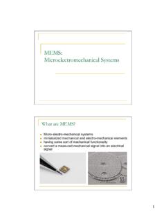
MEMS: Microelectromechanical Systems
courses.cs.washington.eduthis system is its large area ! Compared to a single ring gyro, has much more control over actuation and sensing ! Single rings require flexible support beams as well Why Cut the Circles? •With full concentric circles, the structure tends to be rigid •By using arcs instead, the structure becomes more flexible,

Chemical Resistance and Chemical Applications for CPVC ...
www.nrc.govstrength bleach applications or metal pickling and plating baths. However, no material is without its limitations. In excess of its recommended TPC limits, hot concentrated sulfuric acid may cause blackening and blistering, while hot concentrated nitric …
Adper™ Single Bond 2 Adhesive
multimedia.3m.com5 Introduction Product Description Adper™ Single Bond 2 Adhesive, based on the clinically proven Adper™ Single Bond Adhesive is a total etch, visible-light activated dental bonding agent incorporating 10 percent by weight of 5nm diameter silica filler.