1 100 transistor
Found 9 free book(s)
14. Transistor Characteristics Lab - hunter.cuny.edu
www.hunter.cuny.eduExample: Suppose b=100 and Ib = 1.5 ma. How large is Ic? b = 100.; Ib = 1.5; Ic = b*Ib 150. Obviously the collector current is much larger than the base current. pnp Transistor When the two n regions are next to each other (as below) then one has a pnp transistor. It should be clear that one of the diodes in a transistor is in the forward ...

Complementary low voltage transistor - STMicroelectronics
www.st.comMay 2008 Rev 5 1/9 9 BD135 - BD136 BD139 - BD140 Complementary low voltage transistor Features Products are pre-selected in DC current gain Application General purpose Description These epitaxial planar transistors are mounted in

14 nm Process Technology: Opening New Horizons - Intel
www.intel.com1 10 100 1000 10000 0.001 0.01 0.1 1 10 1970 1980 1990 2000 2010 2020 Micron ~0.7x per nm generation. 22 nm 32 nm 14 nm . Intel Scaling Trend . 7 . Scaled transistors provide: • Higher performance • Lower power • Lower cost per transistor . Moore’s Law continues!
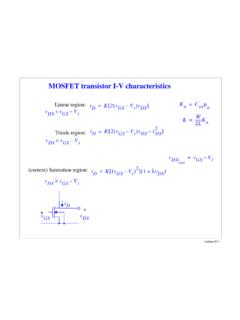
MOSFET transistor I-V characteristics - ECE:Course Page
course.ece.cmu.eduLecture 20-8 PMOSFETs • All of the voltages are negative • Carrier mobility is about half of what it is for n channels p+ n S G D B p+ • The bulk is now connected to the most positive potential in the circuit • Strong inversion occurs when the channel becomes as p-type as it was n-type • The inversion layer is a positive charge that is sourced by the larger potential

Features Mechanical Data - Diodes Incorporated
www.diodes.com40V NPN SMALL SIGNAL TRANSISTOR IN SOT23 Features ... 10m 100m 1 10 100 1k 0.1 1 10 Single Pulse. T amb =25°C Pulse Power Dissipation) Pulse Width (s) 0.001 0.01 0.1 1 0.1 1 10 100 V , COLLECTOR-EMITTER VOLTAGE (V) CE I, C O L L E C T O R C U R R E N T (A) C Fig. 5 Typical Collector Current vs. Collector-Emitter Voltage DC

BC546DB - Amplifier Transistors, NPN Silicon
www.onsemi.com1.0 10 505.0 100 vce = 5 v ta = 25°c c, capacitance (pf) f, current-gain - bandwidth product t 0.5 5.0 20 ta = 25°c cob cib. bc546b, bc547a, b, c, bc548b, c www.onsemi.com 5 …

FQP30N06L 60V LOGIC N-Channel MOSFET - SparkFun …
cdn.sparkfun.comFQP30N06L ©2001 Fairchild Semiconductor Corporation Rev. A1. May 2001 10-5 10-4 10-3 10-2 10-1 100 101 10-2 10-1 100 ※ Notes : 1. Z θ JC (t) = 1.90 ℃ /W Max. 2. Duty Fac tor, D=t

ECE 547 - UNIVERSITY OF MAINE 1 8-Bit Arithmetic Logic Unit
ece.umaine.eduECE 547 - UNIVERSITY OF MAINE 2 I. INTRODUCTION A. Project Overview THE ECE 547 VLSI design project described in this paper is an 8-bit Arithmetic Logic Unit (ALU).We used the 74S181 [1] 4-bit ALU design, which was manufactured by Texas Instruments, as …
Electrons and Holes in Semiconductors - Chenming Hu
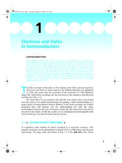
www.chu.berkeley.eduFigure 1–3 introduces a useful system of denoting the orientation of the silicon crystal. The cube in Fig. 1–3a repres ents the Si unit cell shown in Fig. 1–2 and each darkened surface is a crystal plane. The (100) crystal plane in the leftmost drawing in Fig. 1–3a, for example, is simply the plane in Fig. 1–2 closest to the reader.