Transconductance
Found 9 free book(s)
ZVP2106A P-channel enhancement mode vertical DMOS FET ...
www.diodes.comTransconductance v drain current ID- Drain Current (Amps) g fs-T ra n sc o ndu c t a ductance (mS) 0 Q-Charge (nC) Transconductance v gate-source voltage VGS-Gate Source Voltage (Volts) f s-T rans c n 0-10 -20 -30 VDS-Drain Source Voltage (Volts) Capacitance v drain-source voltage C-Capacitance (pF) Coss V G S-Gate Sou r ce V oltag e (V o lts ...

Lecture 17: Common Source/Gate/Drain Amplifiers
inst.eecs.berkeley.eduGeneric Transconductance Amp. Department of EECS University of California, Berkeley EECS 105Fall 2003, Lecture 17 Prof. A. Niknejad Two-Port CS Model Reattach source and load one-ports: Department of EECS University of California, Berkeley EECS 105Fall 2003, Lecture 17 Prof. A. …
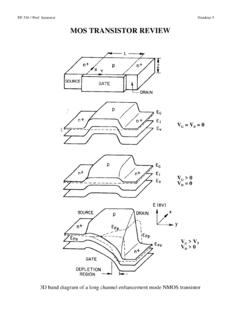
MOS TRANSISTOR REVIEW - Stanford University
web.stanford.edu3. Improve current drive (transconductance gm) g I V V const W L K t V V linear region W L K t V V V saturation region m D G D n ox ox DD n ox ox GT D SAT SAT = = ≈< ≈−()> ∂ ∂ µ µ for V for V D D,, Decreasing the channel length and gate oxide thickness increases gm, i.e., the current drive of the transistor. Much of the scaling is ...

ZVN3310A N-channel enhancement mode vertical DMOS FET ...
www.diodes.comTransconductance v drain current ID- Drain Current (Amps) g f s-T ransconductance (mS) g f s-T rans c o n ducta n ce (m S) 0 80 0 40 120 160 VDS= 25V 0.2 0.4 0.6 0.8 1.0 1.2 0 80 0 40 120 160 VDS= 25V 24 6 8 10 12 VDS-Drain Source Voltage (Volts) Capacitance v drain-source voltage C-p a c ita nce (pF) Coss Ciss Crss 0 10 20 30 40 50 0 30 20 10 ...

LM324 - Single Supply Quad Operational Amplifiers
www.onsemi.comThe transconductance reduction is accomplished by splitting the collectors of Q20 and Q18. Another feature of this input stage is that the input common mode range can include the negative supply or ground, in single supply operation, without saturating either the input

Measuring Power MOSFET Characteristics
www.vishay.comThis is the forward transconductance of the device at a specified value of ID. gfs represents the signal gain (drain current divided by gate voltage) in the linear region. This parameter should be measured with a small AC superimposed on a gate bias an d the curve tracer is not the appropriate tool for this measurement. Even with specific
Transconductance - University of Arizona
atlas.physics.arizona.eduTransconductance 1 Transconductance Transconductance is the property of certain electronic components. Conductance is the reciprocal of resistance; transconductance is the ratio of the current change at the output port to the voltage change at the input port.

30V P-Channel MOSFET
aosmd.comAO3401A Symbol Min Typ Max Units BV DSS-30 V VDS =-30V, V GS =0V -1 TJ=55°C -5 IGSS ±100 nA VGS(th) Gate Threshold Voltage -0.5 -0.9 -1.3 V ID(ON)-27 A 41 50 TJ=125°C 62 75 47 60 mΩ 60 85 mΩ gFS 17 S VSD-0.7 -1 V IS-2 A Ciss 645 pF Coss 80 pF Crss 55 pF Rg 4 7.8 12 Ω Qg(10V) 14 nC Qg(4.5V) 7 nC Qgs 1.5 nC Qgd 2.5 nC tD(on) 6.5 ns tr 3.5 ns tD(off) 41 ns tf …

Power MOSFET
www.vishay.comIRF530 www.vishay.com Vishay Siliconix S21-0819-Rev. C, 02-Aug-2021 1 Document Number: 91019 For technical questions, contact: hvm@vishay.com THIS DOCUMENT IS SUBJECT TO CHANGE WITHOUT NOTICE.