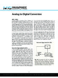
Analog to Digital Conversion - mccdaq.com
input of 10 VDC can resolve the measurement into 10 VDC/4096 = 0.00244 VDC = 2.44 mV. Similarly, for the same 0 to 10 VDC range, a 16-bit ADC resolution is 10/216 = 10/65,536 = 0.153 mV. The resolution is usually specified with respect to the full-range reading of the ADC, not with respect to the measured value at any particular instant.
Download Analog to Digital Conversion - mccdaq.com

Information
Domain:
Source:
Link to this page:
Documents from same domain
Analog to Digital Conversion - Measurement …
www.mccdaq.com2 Measurement Computing • 10 Commerce Way • Norton, MA 02766 • (508) 946-5100 • info@mccdaq.com • mccdaq.com Voltage-to-Frequency ADCs
Data Acquisition Fundamentals - Measurement …
www.mccdaq.comPage 4 Measurement Computing | 1-800-234-4232 | info@mccdaq.com | mccdaq.com coeffi cient, which in turn depends on the chemical composition

USB Voltage and Current Output Devices
www.mccdaq.comMeasurement Computing 3(50) 46-5100 info@mccdaq.com mccdaq.com USB-3100 Series Block Diagrams Microcontroller DIO 8 Channels SPI Full-Speed USB 2.0 Compliant Interface SYNCLD 1 1 ...
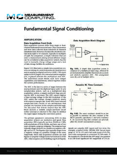
Fundamental Signal Conditioning - Measurement …
www.mccdaq.com3 Measurement Computing • 10 Commerce Way • Norton, MA 02766 • (508) 946-5100 • info@mccdaq.com • mccdaq.com A – + R f 100 kW 0 A
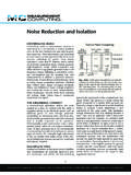
Noise Reduction and Isolation - mccdaq.com
www.mccdaq.comMeasurement Computing • 10 Commerce Way • Norton, MA 02766 • (508) 946-5100 • info@mccdaq.com • mccdaq.com 1 Hot phase A

Saving DASYLab data to an ASCII (text) readable file
www.mccdaq.comDASYLab Techniques Saving DASYLab data to an ASCII (text) readable file Updated to reflect changes in DASYLab 2016 (V14) The DASYLab Getting Started Guide (Manual.pdf is included on the CD and in the Windows Start menu) provides
Fundamental Signal Conditioning - mccdaq.com
www.mccdaq.comfollower and the difference amplifier. Inverting Amplifier Stages The inverter stage is the most basic operational amplifier configuration. It simply accepts an input signal referenced to common, amplifies it, and inverts the polarity at the output terminals. The open-loop gain of a typical operational amplifier is in the hundreds of thousands.

DASYLab - mccdaq.com
www.mccdaq.comDASYLab 2020 . dasylab.com . DASYLab 2020 . Data Acquisition, Controlling, and Monitoring . Sept 2019 324212E-01
Data Acquisition Handbook
www.mccdaq.comMeasurement Computing (508) 946-5100 info@mccdaq.com mccdaq.com Measurement Computing (508) 946-5100 info@mccdaq.com mccdaq.com Data Acquisition Handbook v …
Related documents
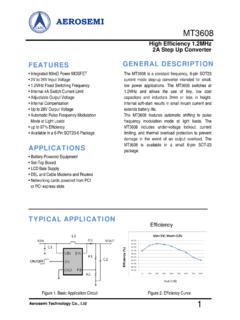
AEROSEMI - Olimex
www.olimex.comInput and Output capacitors should be placed close to the IC and connected to ground plane to reduce noise coupling. The GND should be connected to a strong ground plane for heat sinking and noise protection. Keep the main current traces as possible as short and wide. SW node of DC-DC converter is with high frequency voltage swing.

LF353-NWide Bandwidth Dual JFET Input Operational Amplifier
www.ti.com• Fast Settling Time to 0.01%: 2 μs input offset voltage, low input bias current, high input impedance, high slew rate and wide bandwidth. The devices also exhibit low noise and offset voltage drift. Typical Connection 1 Please be aware that an important notice concerning availability, standard warranty, and use in critical applications of

KAAP686 Mathematics and Signal Processing for …
www1.udel.eduApr 27, 2011 · The rectified signal is low pass filtered, with in the 5 – 100 Hz range, and the result looks like the “envelope” of the original signal. One way to low pass filter a signal is to simply take the mean value, in a window which “slides” along the signal. Some authors advocate this “rectify and mean” approach. Such a moving–average
SECTION 4 SWITCHED CAPACITOR VOLTAGE CONVERTERS …
www.analog.comSwitched capacitor voltage converters do not maintain high efficiency for a wide range of ratios of input to output voltages, unlike their switching regulator counterparts. Because the input to output current ratio is scaled according to the basic voltage conversion (i.e., doubled for a doubler, inverted for an inverter)

LM339 - Single Supply Quad Comparators
www.onsemi.com• Low Input Bias Current: 25 nA (Typ) • Low Input Offset Current: ±5.0 nA (Typ) • Low Input Offset Voltage • Input Common Mode Voltage Range to GND • Low Output Saturation Voltage: 130 mV (Typ) @ 4.0 mA • TTL and CMOS Compatible • ESD Clamps on the Inputs Increase Reliability without Affecting Device Operation
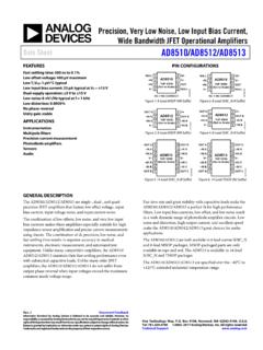
Precision, Very Low Noise, Low Input Bias Current, Wide ...
www.analog.comoutput phase reversal when input voltages exceed the maximum common-mode voltage range. Fast slew rate and great stability with capacitive loads make the AD8510/AD8512/AD8513 a perfect fit for high performance filters. Low input bias currents, low offset, and low noise result in a wide dynamic range of photodiode amplifier circuits. Low
ICM7555 General purpose CMOS timer
www.nxp.comn Wide operating supply voltage range guaranteed 3 V to 16 V over full automotive temperatures n Normal reset function; no crowbarring of supply during output transition ... VI input voltage TRIGGER: VDD = 5 V 0.29VDD 0.31VDD 0.34VDD V CONTROL_VOLTAGE: VDD = 5 V 0.62VDD 0.65VDD 0.67VDD V THRESHOLD: ...

LM2576 - 3.0 A, 15 V, Step-Down Switching Regulator
www.onsemi.com• Adjustable Version Output Voltage Range, 1.23 to 37 V ±4% Maximum Over Line and Load Conditions • Guaranteed 3.0 A Output Current • Wide Input Voltage Range • Requires Only 4 External Components • 52 kHz Fixed Frequency Internal Oscillator • TTL Shutdown Capability, Low Power Standby Mode • High Efficiency