Transcription of Precision, Very Low Noise, Low Input Bias Current, Wide ...
1 Precision, Very Low Noise, Low Input Bias Current, wide Bandwidth JFET Operational AmplifiersDate Sheet AD8510/AD8512/AD8513 Rev. J Document Feedback Information furnished by Analog Devices is believed to be accurate and reliable. However, no responsibility is assumed by Analog Devices for its use, nor for any infringements of patents or other rights of third parties that may result from its use. Specifications subject to change without notice. No license is granted by implication or otherwise under any patent or patent rights of Analog Devices. Trademarks and registered trademarks are the property of their respective owners.
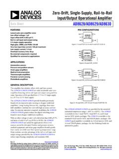
2 One Technology Way, Box 9106, Norwood, MA 02062-9106, : 2002 2017 Analog Devices, Inc. All rights reserved. Technical Support FEATURES Fast settling time: 500 ns to Low offset voltage : 400 V maximum Low TCVOS: 1 V/ C typical Low Input bias current: 25 pA typical at VS = 15 V Dual-supply operation: 5 V to 15 V Low noise: 8 nV/ Hz typical at f = 1 kHz Low distortion: No phase reversal Unity gain stable APPLICATIONS Instrumentation Multipole filters Precision current measurement Photodiode amplifiers Sensors Audio PIN CONFIGURATIONS AD8510 TOP VIEW(Not to Scale)NULL IN+INV NCV+OUTNULL02729-003NC = NO CONNECT12345678AD8510 TOP VIEW(Not to Scale)NULL IN+INV NCV+OUTNULL02729-004NC = NO CONNECT12345678 Figure 1.
3 8-Lead MSOP (RM Suffix) Figure 2. 8-Lead SOIC_N (R Suffix) AD8512 OUT A IN A+IN AV V+OUT B IN B+IN BTOP VIEW(Not to Scale)02729-00112345678AD8512 TOP VIEW(Not to Scale)OUT A IN A+IN AV V+OUT B IN B+IN B02729-00212345678 Figure 3. 8-Lead MSOP (RM Suffix) Figure 4. 8-Lead SOIC_N (R Suffix) AD8513 TOP VIEW(Not to Scale)OUT A1 IN A2+IN A3V+4+IN B5 OUT D IN D+IN DV +IN C1413121110 IN B6 OUT B7 IN COUT C9802729-005AD8513 TOP VIEW(Not to Scale)OUT A IN A+IN AV++IN BOUT D IN D+IN DV +IN C IN BOUT B IN COUT C02729-0061234514131211106798 Figure 5. 14-Lead SOIC_N (R Suffix) Figure 6. 14-Lead TSSOP (RU Suffix) GENERAL DESCRIPTION The AD8510/AD8512/AD8513 are single-, dual-, and quad-precision JFET amplifiers that feature low offset voltage , Input bias current, Input voltage noise, and Input current noise.
4 The combination of low offsets, low noise, and very low Input bias currents makes these amplifiers especially suitable for high impedance sensor amplification and precise current measurements using shunts. The combination of dc precision, low noise, and fast settling time results in superior accuracy in medical instruments, electronic measurement, and automated test equipment. Unlike many competitive amplifiers, the AD8510/ AD8512/AD8513 maintain their fast settling performance even with substantial capacitive loads. Unlike many older JFET amplifiers, the AD8510/AD8512/AD8513 do not suffer from output phase reversal when Input voltages exceed the maximum common-mode voltage range.
5 Fast slew rate and great stability with capacitive loads make the AD8510/AD8512/AD8513 a perfect fit for high performance filters. Low Input bias currents, low offset, and low noise result in a wide dynamic range of photodiode amplifier circuits. Low noise and distortion, high output current, and excellent speed make the AD8510/AD8512/AD8513 great choices for audio applications. The AD8510/AD8512 are both available in 8-lead narrow SOIC_N and 8-lead MSOP packages. MSOP-packaged parts are only available in tape and reel. The AD8513 is available in 14-lead SOIC_N and TSSOP packages. The AD8510/AD8512/AD8513 are specified over the 40 C to +125 C extended industrial temperature range.
6 AD8510/AD8512/AD8513 Date Sheet Rev. J | Page 2 of 20 TABLE OF CONTENTS Features .. 1 Applications .. 1 Pin Configurations .. 1 General Description .. 1 Revision History .. 2 Specifications .. 3 Electrical Characteristics .. 4 Absolute Maximum Ratings .. 6 ESD Caution .. 6 Typical Performance Characteristics .. 7 General Application Information .. 13 Input Overvoltage Protection .. 13 Output Phase Reversal .. 13 Total Harmonic Distortion (THD) + Noise .. 13 Total Noise Including Source Resistors .. 13 Settling Time .. 14 Overload Recovery Time .. 14 Capacitive Load Drive .. 14 Open-Loop Gain and Phase Response.
7 15 Precision 16 I-V Conversion Applications .. 17 Outline Dimensions .. 19 Ordering Guide .. 20 REVISION HISTORY 6/2017 Rev. I to Rev. J Changes to Figure 14 Caption .. 8 Deleted Figure 39; Renumbered 12 Updated Outline Dimensions .. 19 Changes to Ordering Guide .. 20 2/2009 Rev. H to Rev. I Changes to Figure 25 .. 10 Changes to Ordering Guide .. 20 10/2007 Rev. G to Rev. H Changes to Crosstalk Section .. 18 Added Figure 58 .. 18 6/2007 Rev. F to Rev. G Changes to Figure 1 and Figure 2 .. 1 Changes to Table 1 and Table 2 .. 3 Updated Outline Dimensions .. 19 Changes to Ordering Guide.
8 20 6/2006 Rev. E to Rev. F Changes to Figure 23 .. 9 Updated Outline Dimensions .. 19 Changes to Ordering Guide .. 20 6/2004 Rev. D to Rev. E Changes to Format .. Universal Changes to Specifications .. 3 Updated Outline Dimensions .. 19 10/2003 Rev. C to Rev. D Added AD8513 Model .. Universal Changes to Specifications .. 3 Added Figure 36 through Figure 40 .. 10 Added Figure 55 and Figure 57 .. 17 Changes to Ordering Guide .. 20 9/2003 Rev. B to Rev. C Changes to Ordering Guide .. 4 Updated Figure 2 .. 10 Changes to Input Overvoltage Protection Section .. 10 Changes to Figure 10 and Figure 11.
9 12 Changes to Photodiode Circuits 13 Changes to Figure 13 and Figure 14 .. 13 Deleted Precision Current Monitoring Section .. 14 Updated Outline Dimensions .. 15 3/2003 Rev. A to Rev. B Updated Figure 5 .. 11 Updated Outline Dimensions .. 15 8/2002 Rev. 0 to Rev. A Added AD8510 Model .. Universal Added Pin Configurations .. 1 Changes to Specifications .. 2 Changes to Ordering Guide .. 4 Changes to TPC 2 and TPC 3 .. 5 Added TPC 10 and TPC 12 .. 6 Replaced TPC 20 .. 8 Replaced TPC 27 .. 9 Changes to General Application Information Section .. 10 Changes to Figure 5 .. 11 Changes to I-V Conversion Applications Section.
10 13 Changes to Figure 13 and Figure 14 .. 13 Changes to Figure 17 .. 14 Date Sheet AD8510/AD8512/AD8513 Rev. J | Page 3 of 20 SPECIFICATIONS @ VS = 5 V, VCM = 0 V, TA = 25 C, unless otherwise noted. Table 1. Parameter Symbol Conditions Min Typ Max Unit Input CHARACTERISTICS Offset voltage (B Grade)1 VOS mV 40 C < TA < +125 C mV Offset voltage (A Grade) VOS mV 40 C < TA < +125 C mV Input Bias Current IB 21 75 pA 40 C < TA < +85 C nA 40 C < TA < +125 C nA Input Offset Current IOS 5 50 pA 40 C < TA < +85 C nA 40 C < TA < +125 C nA Input Capacitance Differential pF Common Mode pF Input voltage Range + V Common-Mode Rejection Ratio CMRR VCM = V to + V 86 100 dB Large-Signal voltage Gain AVO RL = 2 k , VO = 3 V to +3 V 65 107 V/mV Offset voltage Drift (B Grade)1 VOS/ T 5 V/ C Offset voltage Drift (A Grade)
