
Chapter 11 Differential Amplifier Circuits
differential amplifier of the input part of an operational amplifier. It is used to provide high voltage gain and high common mode rejection ratio. It has other characteristics such as very high input impedance, very low offset voltage and very low input bias current. Differential amplifier can operate in two modes namely common mode and
Download Chapter 11 Differential Amplifier Circuits

Information
Domain:
Source:
Link to this page:
Documents from same domain

Chapter 4 Junction Field Effect Transistor Theory …
staff.utar.edu.my4 Junction Field Effect Transistor Theory and Applications - 114 - Between point A and B, it is the ohmic region of the JFET. It is the region where the voltage and current relationship follows ohm's law.

Chapter 16 Oscillator Circuits and Applications
staff.utar.edu.mywhere A V is the voltage gain of the amplifier and β = V Vout f is the feedback ... Many oscillators are designed utilizing RC network and resistor divider circuits. RC network is basically used to determine the resonant frequency of the oscillator, whilst resistor divider circuit is used to provide attenuated feedback. ...
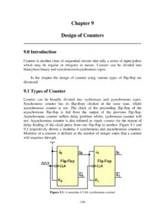
Chapter 9 Design of Counters - Universiti Tunku Abdul Rahman
staff.utar.edu.my09 Design of Counters - 116 - Based on the results obtained from the Karnaugh maps, the circuit design of synchronous decade counter is shown in Fig. 9.15. Figure 9.15: A synchronous decade counter designed using JK flip-flop 9.4.2 Design of an …

Chapter 5 Physics of MOSFET and MOSFET Modeling
staff.utar.edu.my5 Physics of MOSFET and MOSFET Modeling - 88 - where N A is the acceptor doping concentration for p-type semiconductor, ni is the intrinsic carrier concentration and kT/q is the thermal voltage. Substituting equation (5.2) into equation (5.1) yields equation (5.3).

Chapter 16 Fourier Series Analysis
staff.utar.edu.myA rectified half sine wave is defined over one period f(t) = Asin ωt for 0 < t < T/2 and f(t) = 0 for T/2 < t < T as shown in Fig. 16.1. Find the Fourier series of this wave form. Figure 16.1: A half-wave rectifier Solution The dc voltage shall be a 0 = ∫ ω + ∫ T T / 2 T / 2 0 0dt T 1 Asin tdt T 1 = π = − ω ω − A 1 2 T cos T A. The
Related documents

2.7V to 5.5V Single Supply CMOS Op Amp
ww1.microchip.comOct 05, 2007 · Differential Input Impedance ZDIFF — 1013||3 — Ω||pF Common Mode Common Mode Input Range VCMR VSS – 0.3 — VDD – 1.2 V Common Mode Rejection Ratio CMRR 75 90 — dB VDD = 5.0V, VCM = -0.3V to 3.8V Open-loop Gain DC Open-loop Gain (large signal) AOL 100 115 …

Low Distortion, Differential ADC Driver Data Sheet AD8138
www.analog.comThe differential output of the . AD8138 helps balance the input to differential ADCs, maximizing the performance of the ADC. The . AD8138. eliminates the need for a transformer with high performance ADCs, preserving the low frequency and dc infor-mation. The common-mode level of the differential output is adjustable by a voltage on the V OCM

PXIe-4464 Specifications - National Instruments
www.ni.comInput Impedance Configuration Differential Pseudodifferential Between positive input andchassis ground 1 MΩ || 265 pF 1 MΩ || 265 pF Between negative input andchassis ground 1 MΩ || 265 pF 50Ω Gain (dB) DC-Coupled CMRR (dBc)*, † AC-Coupled CMRR (dBc)†, ‡ 30 105 20 100 90 10 90 0 80 80-10, -20 60 75 * f in ≤ 1kHz. † Differential ...

Low Noise Single-Ended to Differential
www.analog.comSingle-Ended to Differential Converter/ADC Driver The LT®6350 is a rail-to-rail input and output low noise single-ended to differential converter/ADC driver featuring fast settling time. It converts a high or low impedance, single-ended input signal to a low impedance, balanced, differential output suitable for driving high performance
Basic Amplifiers and Differential Amplifier
www.cse.psu.eduDifferential Amplifier CSE 577 Spring 2011 Insoo Kim, Kyusun Choi Mixed Signal CHIP Design Lab. Department of Computer Science & Engineering ... High input impedance Low output impedance 2/22/2011 Insoo Kim. Differential Amplifier Single …

Fully-Differential Amplifiers (Rev. E) - TI.com
www.ti.comdifferential signaling is becoming popular in high-speed data acquisition, where the ADC’s inputs are differential and a differential amplifier is needed to properly drive them. Two other advantages of differential signaling are reduced even …

MiCOM P543; P544; P545 & P546 - Current Differential ...
na.eventscloud.comHigh set differential setting (P543 and P545) 2.1.4.7 6-13 Heading and paragraph one amended 2.8.4 Restricted earth fault protection 6-39 New section Setting guidelines for high impedance Restricted Earth fault (REF) 2.8.4.1 6-39 New section 2.18.4.2 6-19 Use of METROSIL non-linear resistors New section 2.17 Integral intertripping

Project Report A 5.2 GHz Differential Cascode Low Noise ...
images.template.netFourth Year Engineering Project Final Report Noah Moser 1 1.0 Introduction The purpose of this project was the design of a Low Noise Amplifier (LNA) at 5.2 GHz

EJA210E Flange Mounted Differential Pressure Transmitter
web-material3.yokogawa.comdifferential pressure and static pressure is also available. Signal Characterizer (Output signal code D, J and Q) ... 1 MΩ or greater (meter input impedance) Note that with three-wire connection, the cable length may affect the measurement accuracy of the output signal.