
EEC 116 Lecture #5: CMOS Logic
Equivalent Inverter • CMOS gates: many paths to Vdd and Gnd – Multiple values for V M, V IL, V IH, etc – Different delays for each input combination • Equivalent inverter – Represent each gate as an inverter with appropriate device width – Include only transistors which are on or switching –Cacualelt V M, delays, etc using ...
Download EEC 116 Lecture #5: CMOS Logic

Information
Domain:
Source:
Link to this page:
Documents from same domain

COMPUTER ORGANIZATION: Architecture - UC …
www.ece.ucdavis.eduCOMPUTER ORGANIZATION: Architecture V. G. Oklobdzija 3 Separation of the machine architecture from implementation enabled several embodiment
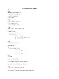
EEC180A Homework 1 Solution 2.5(a) …
www.ece.ucdavis.eduEEC180A Homework 1 Solution Chapter 2 2.5(a) (A+B)(B+C)(B+D’)(ACD’+E) = (B+CA)(B+D’)(ACD’+E) = (B+ACD’)(ACD’+E) = ACD’ + BE 2.5(b)
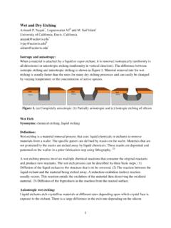
Wet and Dry Etching - University of California, Davis
www.ece.ucdavis.eduSilicon dioxide or silicon nitride is usually used as a masking material against HNA. As the reaction takes place, the material is removed laterally at a rate similar to the speed of etching downward. This lateral and downward etching process takes places even with isotropic
EEC 216 Lecture #1: CMOS Power Dissipation and Trends
www.ece.ucdavis.eduJan 06, 2005 · R. Amirtharajah, EEC216 Winter 2008 5 Why Power Matters • Packaging costs • Power supply rail design • Chip and system cooling costs • Noise immunity and system reliability • Battery life (in portable systems) • Environmental concerns – Office equipment accounted for 5% of total US commercial energy usage in 1993

EEC 216 Lecture #8: Leakage - University of California, Davis
www.ece.ucdavis.edu2. Design a combinational logic datapath at the gate level to compute some function and derive the activity factors of the circuit nodes 3. Design at the transistor level a complex gate, size it based on RC models, and derive worst case switched capacitance 4. Estimate interconnect capacitance and minimize interconnect power 5.
VERILOG 3: TIME AND DELAY - University of California, Davis
www.ece.ucdavis.edu3 Realms of Time and Delay 1) Verilog simulation: “wall clock” time 2) Verilog simulation: timing within the simulation a) These delays are set by “#” delays discussed in the ... Concurrent Operation •Think of verilog modules as operating on independent circuits ...
VERILOG 6: DECODER DESIGN EXAMPLES
www.ece.ucdavis.eduDecoder Design Using Predecoding •Example: 256-output (8 input bits) with predecode –Ex: take groups of 2 input bits •Four possibilities; activate one of four wires (use 2 INVs, 4 ANDs) –Wires along array: 22 * (8/2) = 4 groups of 4 = 16 (same as non-predecoded) –Each output uses a 4-input AND gate (much faster)
Related documents

chapter5.fm Page 144 Monday, September 6, 1999 11:41 AM
bwrcs.eecs.berkeley.eduTHE CMOS INVERTER Quantification of integrity, performance, and energy metrics of an inverter Optimization of an inverter design 5.1 Introduction 5.2 The Static CMOS Inverter — An Intuitive Perspective 5.3 Evaluating the Robustness of the CMOS Inverter: The Static Behavior 5.3.1 Switching Threshold 5.3.2 Noise Margins 5.3.3 Robustness Revisited

DESIGNING COMBINATIONAL LOGIC GATES IN CMOS
bwrcs.eecs.berkeley.edu6.2Static CMOS Design The most widely used logic style is static complementary CMOS. The static CMOS style is really an extension of the static CMOS inverter to multiple inputs.In review, the pri- mary advantage of the CMOS structure is robustness (i.e, low sensitivity to noise), good

Lecture 13 - MIT
web.mit.edu2. CMOS inverter: Propagation delay Inverter propagation delay: time delay between input and output signals; figure of merit of logic speed. Typical propagation delays: < 100 ps. ˜Complex logic system has 10-50 propagation delays per clock cycle. Estimation of tp: use square-wave at input Average propagation delay: tp = 1 2 ()tPHL +tPLH V DD V ...

I. CMOS Inverter: Propagation Delay A. Introduction
web.mit.eduI. CMOS Inverter: Propagation Delay A. Introduction • Propagation delays tPHL and tPLH define ultimate speed of logic • Define Average Propagation Delay • Typical complex system has 20-50 propagation delays per clock cycle. • Typical propagation delays < 1nsec B. Hand Calculation • Use an input signal that has tr =0 and tf

CMOS Technology and Logic Gates - MIT OpenCourseWare
ocw.mit.eduCMOS VLSI is thedigital implementation technology of choice for the foreseeable future (next 10-20 years) – Excellent energy versus delay characteristics – High density of wires and transistors – Monolithic manufacturing of devices and interconnect, cheap! 6.884 – Spring 2005 2/07/2005 L03 – CMOS Technology 4
CMOS Inverter: DC Analysis
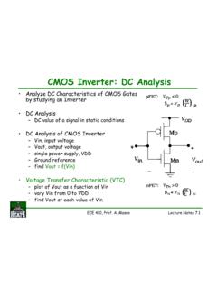
www.egr.msu.eduCMOS Inverter: DC Analysis • Analyze DC Characteristics of CMOS Gates by studying an Inverter • DC Analysis – DC value of a signal in static conditions • DC Analysis of CMOS Inverter egat lo vtupn i,n–Vi – Vout, output voltage – single power supply, VDD – Ground reference –find Vout = f(Vin) • Voltage Transfer Characteristic ...

CMOS Inverter: DC Analysis
www.egr.msu.eduCMOS Inverter: DC Analysis • Analyze DC Characteristics of CMOS Gates by studying an Inverter s i sy l a An•DC – DC value of a signal in static conditions • DC Analysis of CMOS Inverter – Vin, input voltage – Vout, output voltage VDD,ylppu srew poelgn–si – Ground reference –find Vout = f(Vin) • Voltage Transfer ...

CMOS INVERTER CHARACTERISTICS - idc-online.com
www.idc-online.comA CMOS inverter contains a PMOS and a NMOS transistor connected at the drain and gate terminals, a supply voltage VDD at the PMOS source terminal, and a ground connected at the NMOS source terminal, were VIN is connected to the gate terminals and VOUT is connected to the drain terminals.( given in diagram). It is important to notice that the ...