Example: barber
Lecture 13 - MIT
2. CMOS inverter: Propagation delay Inverter propagation delay: time delay between input and output signals; figure of merit of logic speed. Typical propagation delays: < 100 ps. ˜Complex logic system has 10-50 propagation delays per clock cycle. Estimation of tp: use square-wave at input Average propagation delay: tp = 1 2 ()tPHL +tPLH V DD V ...
Tags:
Information
Domain:
Source:
Link to this page:
Documents from same domain
Wireless Communications and Networks
web.mit.edu4 MIT Physical layer •The physical layer plays a very important role in wireless network because it has severe limitation on transmissions Uplink with respect to downlink
The Aleph - MIT
web.mit.eduThe Aleph by Jorge Luis Borges O God! ... He read me many other stanzas, each of which also won his own approval and elicited his lengthy explications.
Finite Element Method
web.mit.eduRobert Cook, Finite Element Modeling For Stress Analysis, John Wiley & Sons, 1995 Introduction to Finite Element Method, http://210.17.155.47 (in Korean)
Finite Element Analysis
web.mit.eduFinite Element Analysis David Roylance Department of Materials Science and Engineering Massachusetts Institute of Technology Cambridge, MA 02139 February 28, …

TECHNICAL & SERVICE MANUAL - MIT
web.mit.eduwhen wiring electrical shock can cause severe personal injury or death. only a qualified, experienced electrician should attempt to wire this system.
Chapter 21 Rigid Body Dynamics: Rotation and …
web.mit.eduChapter 21 Rigid Body Dynamics: Rotation and ... patience to the establishment of the laws of rotation of the solid ... general treatment of mechanics, ...

5.33 Lecture Notes: Introduction To Polymer …
web.mit.edu5.33 Lecture Notes: Introduction To Polymer Chemistry Polymer: A large molecule (macromolecule) built up by repetitive bonding (covalent) of smaller molecules (monomers) • Generally not a well defined structure, or molecular weight.
UNDERSTANDING, FINDING, & ELIMINATING …
web.mit.edua Senior Member of the Institute of Electrical and Electronic Engineers. CEDIA EST016 UNDERSTANDING, ... GROUNDING, AC POWER, AND SAFETY ...
PRESENTED AT THE 2004 AMERICAN CONTROL …
web.mit.eduPRESENTED AT THE 2004 AMERICAN CONTROL CONFERENCE 1 Internal and External Op-Amp Compensation: A Control-Centric Tutorial ... circuit operational …
Frank and Lillian Gilbreth and the Manufacture and ...
web.mit.eduFrank and Lillian Gilbreth and the Manufacture ... time study, despite its ... publicizing micro-motion study as an advance over time study and as an
Related documents

chapter5.fm Page 144 Monday, September 6, 1999 11:41 AM
bwrcs.eecs.berkeley.eduTHE CMOS INVERTER Quantification of integrity, performance, and energy metrics of an inverter Optimization of an inverter design 5.1 Introduction 5.2 The Static CMOS Inverter — An Intuitive Perspective 5.3 Evaluating the Robustness of the CMOS Inverter: The Static Behavior 5.3.1 Switching Threshold 5.3.2 Noise Margins 5.3.3 Robustness Revisited

DESIGNING COMBINATIONAL LOGIC GATES IN CMOS
bwrcs.eecs.berkeley.edu6.2Static CMOS Design The most widely used logic style is static complementary CMOS. The static CMOS style is really an extension of the static CMOS inverter to multiple inputs.In review, the pri- mary advantage of the CMOS structure is robustness (i.e, low sensitivity to noise), good

I. CMOS Inverter: Propagation Delay A. Introduction
web.mit.eduI. CMOS Inverter: Propagation Delay A. Introduction • Propagation delays tPHL and tPLH define ultimate speed of logic • Define Average Propagation Delay • Typical complex system has 20-50 propagation delays per clock cycle. • Typical propagation delays < 1nsec B. Hand Calculation • Use an input signal that has tr =0 and tf

EEC 116 Lecture #5: CMOS Logic
www.ece.ucdavis.eduEquivalent Inverter • CMOS gates: many paths to Vdd and Gnd – Multiple values for V M, V IL, V IH, etc – Different delays for each input combination • Equivalent inverter – Represent each gate as an inverter with appropriate device width – Include only transistors which are on or switching –Cacualelt V M, delays, etc using ...
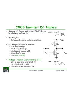
CMOS Inverter: DC Analysis
www.egr.msu.eduCMOS Inverter: DC Analysis • Analyze DC Characteristics of CMOS Gates by studying an Inverter • DC Analysis – DC value of a signal in static conditions • DC Analysis of CMOS Inverter egat lo vtupn i,n–Vi – Vout, output voltage – single power supply, VDD – Ground reference –find Vout = f(Vin) • Voltage Transfer Characteristic ...

CMOS Inverter: DC Analysis
www.egr.msu.eduCMOS Inverter: DC Analysis • Analyze DC Characteristics of CMOS Gates by studying an Inverter s i sy l a An•DC – DC value of a signal in static conditions • DC Analysis of CMOS Inverter – Vin, input voltage – Vout, output voltage VDD,ylppu srew poelgn–si – Ground reference –find Vout = f(Vin) • Voltage Transfer ...

CMOS INVERTER CHARACTERISTICS - idc-online.com
www.idc-online.comA CMOS inverter contains a PMOS and a NMOS transistor connected at the drain and gate terminals, a supply voltage VDD at the PMOS source terminal, and a ground connected at the NMOS source terminal, were VIN is connected to the gate terminals and VOUT is connected to the drain terminals.( given in diagram). It is important to notice that the ...

CMOS Technology and Logic Gates - MIT OpenCourseWare
ocw.mit.eduCMOS VLSI is thedigital implementation technology of choice for the foreseeable future (next 10-20 years) – Excellent energy versus delay characteristics – High density of wires and transistors – Monolithic manufacturing of devices and interconnect, cheap! 6.884 – Spring 2005 2/07/2005 L03 – CMOS Technology 4