
Introduction Differential Traces
W width of a single trace in a differential pair S space between two traces of a differential pair D space between two adjacent differential pairs B thickness of the board For good coupling between two conductors of a differential pair, the following rules should be followed:
Download Introduction Differential Traces

Information
Domain:
Source:
Link to this page:
Documents from same domain
Intel® AMT Configuration Utility User Guide
www.intel.comIntel® AMT Configuration Utility . User Guide . Version 11.0 . Document Release Date: December 17, 2015
Land Grid Array (LGA) Socket and Package …
www.intel.com3. Introduction. In this document, Intel has integrated customer feedback and developed a reference process to serve as a manufacturing enabling solution.
Microcode Revision Guide - intel.com
www.intel.comMicrocode Update Guidance Code Name Product Collection Product Names Vertical Segment CPUID Platform ID OS Update for Q2 Production Status Pre-Mitigation

U.S. Intern Relocation Guide (Including Canada)
www.intel.comFINDING HOUSING You are responsible for arranging your own housing needs, up to and including signing the lease, ordering rental furniture, paying deposits and setting up utilities.
DrMOS Specifications - Intel
www.intel.comTechnical Specifications R 7 3 Technical Specifications The feature set for the DrMOS can be divided into two major areas. They address the electrical
Intel Stratix 10
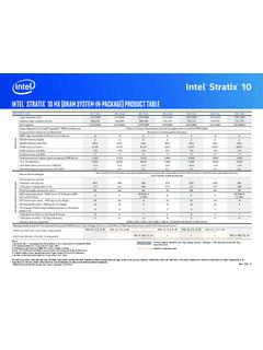
www.intel.comIntel® Stratix® 10 Intel ® StratIx® 10 Mx (DraM SySteM-In-Package) ProDuct table Notes: 1. LE counts valid in comparing across Intel FPGA devices, and …
Intel® Intel® Command Line InterfaceCommand …
www.intel.comIntel® Intel® Command Line InterfaceCommand Line InterfaceCommand Line Interface ... Intel® Command Line Interface Features and ... • Linux* command shell .
Data Sheet: MAX 3000A Programmable Logic …
www.intel.comAltera Corporation 3 MAX 3000A Programmable Logic Device Family Data Sheet The MAX 3000A architecture supports 100 % transistor-to-transistor logic
256 10 GX, MX, TX, and SX Device Family Pin …
www.intel.comIntel® Stratix® 10 GX Pin Connection Guidelines Clock and PLL Pins Note: Intel recommends that you create an Intel ® Quartus Prime design, enter your device I/O assignments, and compile the
256 10 L- and H-Tile Transceiver PHY User Guide - …
www.intel.comIntel® Stratix® 10 L- and H-Tile Transceiver PHY User Guide Subscribe Send Feedback UG-20055 | 2018.07.06 Latest document on the web: PDF | HTML
Related documents

Layout Design Guide - Toradex
docs.toradex.comLayout Design Guide Toradex AG l Altsagenstrasse 5 l 6048 Horw l Switzerland l +41 41 500 48 00 l www.toradex.com l info@toradex.com Page | 2 Issued by: Toradex Document Type: Design Guide Purpose: This document is a guideline for designing a carrier board with high speed signals that is used with Toradex Computer Modules. Document

Board Design Guidelines for PCI Express™ Architecture
e2e.ti.comTrace LengthTrace Length §Longer trace length ⇒ loss ↑ ü~0.25 to 0.35 dB inherent loss per inch for FR4 microstrip traces at 1.25GHz §Manage trace lengths to minimize loss üExample: 12” board, 3.5” add-in card lengths Example VNA measurements for differential mstrip trace insertion loss -5.23dB 1.25GHz 20-inch line freq dB Layout ...

AN-111
ww1.microchip.comDifferential Signal Layout • Differential pair (TX+/- or RX+/-) should be routed away from all other signals and close together to use 5-mil trace width and 5-mil trace space in same length as possible with 100 ohms controlled trace. • Keep both traces of each differential pair as identical to each other as possible.
Routing DDR4 Interfaces Quickly and Efficiently
www.cadence.comDesign rules above are for reference only and should be treated as such—only tried and true way to determine interface design rules is with pre- /post-route simulations DDR4 Design Rules

AN3940, Hardware and Layout Design Considerations for …
www.nxp.comHardware and Layout Design Considerations for DDR3 SDRAM Memory Interfaces, Rev. 6 Freescale Semiconductor 5 DDR3 designer checklist 30. Note: Some product implementations may support only the single-ended version of the strobe. † Match all segment lengths between differential pairs along the entire length of the pair.

AN5097, Hardware and Layout Design Considerations for …
www.nxp.compair. Trace match the MDQS/MDQS pair to be within +/-5 mils. • Maintain constant line impedance along the routing path by maintaining the required line width and trace separation for the given stackup. • Avoid routing differential pairs adjacent to noisy signal lines or high-speed switching devices such as clock chips.
High-Speed Layout Guidelines for Signal Conditioners and ...
www.ti.com3.1 Trace Impedance For high speed signals trace impedance needs to designed as to minimize the reflections in traces. There are two types of trace impedance that need to be taken into consideration when designing high speed signals. Single ended impedance is the trace impedance with reference to ground. Differential Impedance
Xilinx UG393 Spartan-6 FPGA PCB Design Guide
www.xilinx.comSpartan-6 FPGA PCB Design and Pin Planning www.xilinx.com UG393 (v1.3) October 17, 2012 Xilinx is disclosing this user guide, manual, release note, and/ or specification (the "Documentation") to you solely for use in the development