Micron Serial NOR Flash Memory
Micron Serial NOR Flash Memory 3V, Multiple I/O, 4KB Sector Erase N25Q256A Features • SPI-compatible serial bus interface • Double transfer rate (DTR) mode • 2.7–3.6V single supply voltage • 108 MHz (MAX) clock frequency supported for all protocols in single transfer rate (STR) mode • 54 MHz (MAX) clock frequency supported for all
Download Micron Serial NOR Flash Memory

Information
Domain:
Source:
Link to this page:
Documents from same domain

Micron Serial NOR Flash Memory
www.micron.comMicron Serial NOR Flash Memory 3V, Multiple I/O, 4KB, 32KB, 64KB, Sector Erase MT25QL128ABA Features • SPI-compatible serial bus interface • Single and double transfer rate (STR/DTR)
TN-40-07: Calculating Memory Power for DDR4 SDRAM
www.micron.comThis technical note details how DDR4 SDRAM consumes power and provides the tools ... TN-40-07: Calculating Memory Power for DDR4 SDRAM Introduction CCM005-524338224-10497 Rev. B 8/18 EN 1 ... (XXX), where XXX is the subcomponent power.) 2. Derate the power based on the command scheduling in the system (Psch[XXX]).
2Gb NAND Flash Memory - Micron Technology
www.micron.com2, 4, 8Gb: x8/x16 Multiplexed NAND Flash Memory List of Figures PDF: 09005aef818a56a7 / Source: 09005aef81590bdd Micron Technology, Inc., reserves the right to change products or specifications without notice.

TN-46-05 GENERAL DDR SDRAM FUNCTIONALITY …
www.micron.comclock frequency. Therefore, a DDR266 device with a clock frequency of 133 MHz has a peak data transfer rate of 266 Mb/s or 2.1 GB/s for a x64 DIMM. This is ... I/O GATING COLUMN DECODER BANK0 MEMORY ARRAY (4,096 x 1,024 x 8) BANK0 ROW-ADDRESS LATCH AND DECODER 4,096 SENSE AMPLIFIERS BANK CONTROL LOGIC 12 BANK1 BANK2 BANK3 …

TN-ED-03: GDDR6: The Next-Generation Graphics DRAM
www.micron.comFrom the figure above it becomes apparent that the three GDDR standards have many similarities. In fact, taking GDDR5 as the parent GDDR standard, only select items have been modified from the migration of GDDR5 to GDDR5X and GDDR6 to allow as smooth a transition as possible to each next-generation standard.

TN-41-02: DDR3 ZQ Calibration
www.micron.comTechnical Note DDR3 ZQ Calibration Introduction For more robust system operation, the DDR3 SDRAM driver design has been enhanced with reduced capacitance, dynamic on-die termination (ODT), and a new calibration scheme. The capacitance reduction comes from the use of a new “merged” driver. With

Introduction Technical Note - Micron Technology
www.micron.comIntroduction PDF: 09005aef8467c543/Souce: 09005aef8467d772 Micron Technology, Inc., reserves the right to change products or specifications without notice. tn2959_bbm_in_nand_flash.fm - Rev. H 4/11 EN 1 ©2011 Micron Technology, Inc.

TN-41-13: DDR3 Point-to-Point Design Support
www.micron.comVoltage (core, I/O) 1.8V 1.5V Lower power Low power (core, I/O) NA 1.35V Lower power VREF input 1 – all inputs 2 – DQs and CMD/ADDR Improved power delivery Data rate 800 MT/s 1600 MT/s 2X data rate tCK DLL enabled 125–400 MHz 300–800 MHz 2X clock rate tCK DLL disabled Undefined 12.8–125 MHz Slow clock debug Prefetch 4 bits (4n) 8 bits ...

TN-ED-04: GDDR6 Design Guide - Micron Technology
www.micron.comsignal is such that it is always sourced from DRAM to controller, for both reads and writes. Due to this, extra care is recommended during PCB design and analysis ensuring the EDC net is evaluated for both near-end and far-end crosstalk. TN-ED-04: GDDR6 Design Guide GDDR6 Overview CCM005-524338224-10517 tn_ed_04_gddr6_design_guide.pdf - Rev. B ...
Hybrid Memory Cube HMC Gen2 - Micron Technology
www.micron.comHybrid Memory Cube (HMC) is a single package con-taining four DRAM die and one logic die, all stacked together using through-silicon via (TSV) technology. Within each cube, memory is organized vertically— portions of each memory die are combined with the corresponding portions of the other memory die in the stack.
Related documents

Serial Killer Statistics - Radford
maamodt.asp.radford.eduSerial Killer Statistics The tables in this report are based on information from the Radford University/FGCU Serial Killer Database. The purpose of the database is to gather data so that researchers and teachers will have accurate information about serial killers. In 2012, Radford
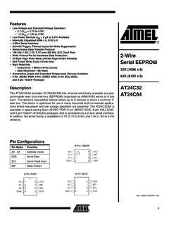
2-Wire Serial EEPROM AT24C32 AT24C64
ww1.microchip.comSCL: Serial Clock, SDA: Serial Data I/O Note: 1. The write cycle time t WR is the time from a valid stop condition of a write sequence to the end of the internal clear/write cycle. twr (1) STOP CONDITION START WORDn 8th BIT ACK SCL SDA. 8 AT24C32/64 0336K–SEEPR–7/03 Data Validity Start and Stop Definition

I2C Serial Interface 20x4 LCD Module - HandsOn Tec
www.handsontec.comI2C Serial Interface 20x4 LCD Module This is I2C interface 20x4 LCD display module, a new high-quality 4 line 20 character LCD module with on-board ... 6 E MPU Operation (data read/write) enable signal 7~10 DB0~DB3 MPU Four low order bi …

JESD204B Survival Guide - Analog Devices
www.analog.comthe serial data link was defined for a single serial lane between a converter or multiple converters and a receiver. A graphical representation is provided in Figure 1. The lane shown is the physical interface between M number of converters and the
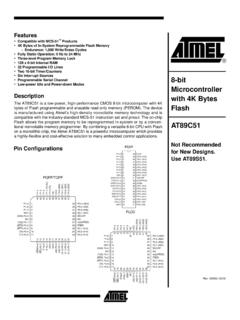
Programmable Serial Channel 8-bit Microcontroller
www.keil.coma full duplex serial port, on-chip oscillator and clock cir-cuitry. In addition, the AT89C51 is designed with static logic for operation down to zero frequency and supports two software selectable power saving modes. The Idle Mode stops the CPU while allowing the RAM, timer/counters, serial port and interrupt system to continue functioning. The

Serial Communications RS232, RS485, RS422
www.raveon.comAn RS232 serial bus consists of just two communication wires - one for sending data and another for receiving. As such, serial devices should have two serial pins: the receiver, RX, and the transmitter, TX. Because the communication data is based upon the voltage on the wires, relative to the ground level, a ground connection must be

Post-War Serial Number Data - Walther P.38 Pistol
www.p-38.infoTitle: Microsoft Word - Post-war serial number data.docx Author: Atarian Created Date: 3/2/2013 8:44:34 PM