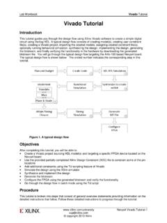
Vivado tutorial - Xilinx
1-1-4. Enter tutorial in the Project name field. Make sure that the Create Project Subdirectory box is checked. Click Next. Figure 3. Project Name and Location entry 1-1-5. Select RTL Project option in the Project Type form, and click Next. 1-1-6. Select Verilog as the Target language and Simulator language in the Add Sources form. 1-1-7.
Download Vivado tutorial - Xilinx

Information
Domain:
Source:
Link to this page:
Documents from same domain

Zynq-7000 All Programmable SoC Software …
www.xilinx.comZynq-7000 All Programmable SoC Software Developers Guide UG821 (v12.0) September 30, 2015

Zynq-7000 SoC Data Sheet: Overview (DS190) - All …
www.xilinx.comZynq-7000 SoC Data Sheet: Overview DS190 (v1.11.1) July 2, 2018 www.xilinx.com Product Specification 3 Programmable Logic Xilinx 7 Series Programmable Logic

7 Series FPGAs Data Sheet: Overview (DS180)
www.xilinx.com7 Series FPGAs Data Sheet: Overview DS180 (v2.6) February 27, 2018 www.xilinx.com Product Specification 2 Spartan-7 FPGA Feature Summary Table 2: Spartan-7 FPGA Feature Summary by Device

Accelerating OpenCV Applications with Zynq-7000 …
www.xilinx.comReference Design XAPP1167 (v3.0) June 24, 2015 www.xilinx.com 2 The design flow for this application note generally follows the steps below: 1. Develop and execute an OpenCV application on Desktop.

Product Obsolete/Under Obsolescence …
www.xilinx.comEfficient Shift Registers, LFSR Counters, and Long Pseudo-Random Sequence Generators 2 XAPP 052 July 7,1996 (Version 1.1) Divide-By 5 to 16 Counter in Two CLBs

XILINX ARTIX-7 FPGAS: A NEW PERFORMANCE …
www.xilinx.comKey Capability Overview . Smallest Package • Low-cost, wire-bond, chip-scale BGA packaging • Available in a 10x10mm package for maximum system integration

Platform Flash In-System Programmable …
www.xilinx.comPlatform Flash In-System Programmable Configuration PROMs DS123 (v2.19) June 6, 2016 www.xilinx.com Product Specification 2 R When the FPGA is in Master Serial mode, it generates a

Spartan-3AN FPGA Family Data Sheet (DS557) - Xilinx
www.xilinx.comSpartan-3AN FPGA Family: Introduction and Ordering Information DS557 (v4.2) June 12, 2014 www.xilinx.com Product Specification 3 Architectural Overview

Xilinx XAPP1113 Designing Efficient Digital Up and …
www.xilinx.comIntroduction XAPP1113 (v1.0) November 21, 2008 www.xilinx.com 2 R • DDC design files for multi-channel MRI, targeting both Virtex-5 and Spartan®-DSP

Xilinx DS060 Spartan and Spartan-XL FPGA …
www.xilinx.comSpartan and Spartan-XL FPGA Families Data Sheet 2 www.xilinx.com DS060 (v2.0) March 1, 2013 Product Specification R Product Obsolete/Under Obsolescence General Overview Spartan series FPGAs are implemented with a regular, flex-
Related documents

Vivado Tutorial - Xilinx
www.xilinx.com1-5. I/O constraints 1-5-1. Once RTL analysis is performed, another standard layout called the I/O Planning layout is available. Click on the drop-down button and select the I/O Planning layout. Figure 10. I/O Planning layout selection Notice that the Package view is displayed in the Auxiliary View area, RTL Netlist tab is selected,
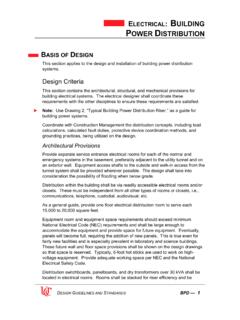
ELECTRICAL B POWER DISTRIBUTION BASIS OF DESIGN
www.uc.eduLab areas will be designed with the capacity of at least 1 power outlet per 30 square feet. Dedicated circuits will be supplied for all refrigerators, centrifuges, and ... – Statement on power distribution system layout and basis of design • Schematic Design Phase – Design requirements and location of electrical rooms and closets

TUTORIAL CADENCE DESIGN ENVIRONMENT - Anasayfa
web.itu.edu.tr11:15H-13:00H: Lab session Schematic Edition and Simulation of an OTA TUESDAY, OCTOBER 22 9:00H-11:00H. Lecture Layout Edition and Verification with Cadence Virtuoso and Diva. 11:00H-11:15H: Break 11:15H-13:00H: Lab session Layout of an OTA. Verification: DRC, LVS, post-layout simulation (First session) WEDNESDAY, OCTOBER 23 9:00H-11:00H. Lecture
Cadence Virtuoso Tutorial - USC Viterbi
ee.usc.eduRemember that when you use more than one symbol in schematic, they all will have common Vdd and Gnd even if there are one Gnd and Vdd for each symbol (in the original design). To design with symbols in layout, you should make sure that all of the Vdd and Gnds are connected.
Heat and Mass Transfer Laboratory Manual
sjce.ac.inLaboratory Layout 1. Critical heat flux apparatus 2. Stefan-Boltzmann unit 3. Thermal conductivity of metal rod 4. Emissivity measurement unit 5. Thermal conductivity of liquid 6. Parallel and counter flow heat exchanger 7. Air conditioning test rig 8. Natural convection heat transfer 9. Heat transfer from Pin-Fin unit 10.
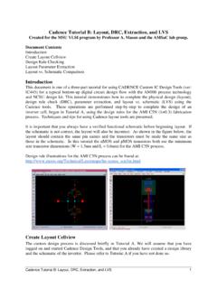
Cadence Tutorial B: Layout, DRC, Extraction, and LVS
www.egr.msu.edudesign rule check (DRC), parameter extraction, and layout vs. schematic (LVS) using the Cadence tools. These operations are performed step-by-step to complete the design of an inverter cell, began in Tutorial A, using the design rules for the AMI C5N (λ=0.3) fabrication process. Techniques and tips for using Cadence layout tools are presented.
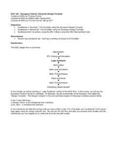
ECE 128 Synopsys Tutorial: Using the Design Compiler ...
s2.smu.edu1) Design Vision- a GUI (Graphical User Interface) 2) dc_shell - a command line interface In this tutorial we will take the verilog code you have written in lab 1 for a full adder and “synthesize” it into actual logic gates using the design compiler tool. We will use the GUI first, and after you become more familiar with the
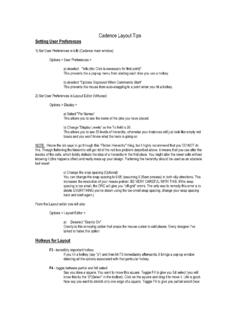
Cadence Layout Tips - Pennsylvania State University
www.cse.psu.eduCadence Layout Tips Setting User Preferences 1) Set User Preferences in icfb (Cadence main window) ... I know the lab says to go through this "Flatten Hierarchy" thing, but I highly recommend that you DO NOT do ... and the file you're trying to look at are not the same. Close the LVS, close the extracted, save the schematic and the layout, then ...