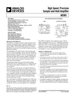
Transcription of A High-Performance, Low-Cost Analog Switch Family
1 AN208 vishay SiliconixDocument Number: FaxBack 408-970-56006-1A high - performance , Low-Cost Analog Switch FamilyIntroductionVishay Siliconix popular DG201 quad Analog Switch has beenan industry workhorse for over two decades. To meet thedemands of new applications for more precision and fasterswitching speeds, an improved version of the DG201, alongwith five other general purpose Analog switches, is beingintroduced by vishay Siliconix. The new B series provideslower Switch on-resistance, leakage current, turn-on time,charge injection, and power consumption at pricescomparable to industry-standard these improved levels of performance isVishay Siliconix new high -voltage silicon gate process,HVSG-II.
2 HVSG-II substantially increases the Switch s overallperformance, allowing Analog signals to be switched efficientlyfrom 20 V to +3 V. Even though these devices were designedon a high -voltage process, they still exhibit very goodlow-voltage performance and provide a single-supply general-purpose parts are ideal for a host ofapplications, including automatic test equipment, instru-mentation, and voice or data communications. This notedetails performance improvements, and provides acompetitive comparison and overview of general Single-Supply OperationThe B Family can be used with split supplies or a singlesupply.
3 The DG201B/202B have an internal +5-V DG211B and DG212B are ideal for low-voltage singlesupply operation (+3 V to +5 V).FIGURE 1. B Series DiagramsINSDTTLor CMOSINSDCMOSINSDDG201 BNormally Closed, Internal RegulatorDG211 BNormally ClosedDG308 BNormally ClosedINSDINSDCMOSINSDDG202 BNormally Open, Internal RegulatorDG212 BNormally OpenDG309 BNormally OpenTTLor CMOSTTLor CMOSTTLor CMOSAN208 vishay FaxBack 408-970-56006-2 Document Number: 7060610-Aug-99 DG211B/212B Typical Low-Voltage PerformanceV+ & VL(V)LogicThreshold(V)tON(ns)tOFF(ns)+5+ + +220050+4+ + + +3+ + + +2+11600400 Note: VS = +2 V, RL =1 k , V = 0 VSimply connect VL to V+ (Figure 2).
4 The voltage at VL sets thelogic threshold (Table 1).Even though the DG211B and DG212B operate as low as+2 V, their turn-on time increases proportionally to thedecrease in V+. At + V these devices are quite suitable forgeneral applications, even though their on-resistance canapproach 1 k . Later it will be shown how this resistance canalso be substantially reduced. The DG201B/202B parts alsowere tested to +3 V with similar performance (except tONwhich was slightly slower).Speed Combined With PowerNormally the speed of an Analog Switch can only be increasedat the expense of the power driving the chip.
5 But the B seriesdevices overcome this problem with reduced channel lengthsand parasitic improvements allow the DG211B s turn-on (tON) time tobe reduced to 120 ns typical, and power dissipation (PD) to beas low as nW during the quiescent condition. Note that bothtON and PD are a function of the power supplies used to powerthe 1 shows the correlation between low voltage effects ofthe supply voltage used. The switching speed is typically120 ns with split 15-V supplies. It slows to 1600 ns with a mere+2-V single supply.
6 Turn-on time (tON) is measured from 50%of the INPUT logic control to 90% of the Analog output interval includes the delay through the logic translator,FET driver stages, and the FETs themselves. An RC timeconstant comprised of the channel on-resistance and theoutput load capacitance (CL) increases tON with an increase inCL. This effect is minimal as long as a shunt resistive load isalso present. The increase in tON is approximately equal to: tON = rDS(on) CLwhere CL is the value above 35 pF (and 35 pF is the standardCL used to measure tON).
7 Low On-ResistanceOn-resistance can make a critical addition to the error budgetin precision applications. For the B devices, typical rDS(on) is45 and is in series with a load resistance RL (Figure 2). Theerror is equal to rDS(on)/(rDS(on) + RL) or 45/(45 + 1 k) = Single-Supply OperationINSDDG211 BGNDV RL1 k V+VL+2 V to +5 VFIGURE Voltage rDS(on) CurvesV+ = +2 V0151500100900700500300VD Drain Voltage (V)rDS(on)() +5 V+4 V+ V+3 V+ V23 413001100AN208 vishay SiliconixDocument Number: FaxBack 408-970-56006-3 Increasing RL will proportionally reduce this error.
8 However, alarge load resistance reduces the off-isolation. If the analogsignal is dc, off-isolation is not a problem since it will not becoupled through the off-channel parasitic capacitor. But if theanalog signal is ac, then the off-isolation decreases as thefrequency increases or if RL increases. One solution to thisproblem is to run the Switch into the virtual ground of aninverting amplifier, as described FlatnessOn-resistance flatness is a measure of the change in rDS(on)when the source or drain voltage varies.
9 This delta can distortthe input signal as follows:Harmonic Distortion+20 log RONRLL imiting Analog signal dynamic range to the flattest part of therDS(on) curve can reduce this error. A virtual ground at thesumming junction of an op amp can provide the highimpedance required to reduce distortion. If the non-invertinginput of an op amp is referenced to ground, a virtual groundappears at the inverting input because the input offset voltage(VOS) of most op amps is in the microvolt or millivolt the inverting input is only the value of this input voltageabove or below ground.
10 This virtual ground node is also a veryhigh impedance point becauseRIN+VOSIB where IB is the input bias current of the op amp. For instance,a typical op amp with VOS = 1 mV and IB = 1 nA would have aninput impedance of 1 M .Bandwidth ImprovementsThe bandwidth of a general-purpose Analog Switch isgenerally not specified on most data sheets. Bandwidth can becalculated by this expression:f 3db+12pRCwhere R = rDS(on) and C = CD(on), also RL assumed to 45 and 16 pF, respectively, results in atheoretical calculated bandwidth of [220 MHz.]