0 Introduction Cmos Vlsi
Found 9 free book(s)
Chapter 1 Introduction to CMOS Circuit Design
www.ee.ncu.edu.twIntroduction to CMOS Circuit Design Jin-Fu Li Advanced Reliable Systems (ARES) Lab. ... A=0 Mn Off V DD V A V Tn 0 Logic translation V A V GSn Drain Mn Source Gate-source voltage Gate +-V A=1 Mp Off V A=0 Mp On V DD V A V ... Design Flow for a VLSI Chip Specification Behavioral Design Structural Design Physical Design Function Function Function ...
Course Offering UG 2nd Year and Rest, Monsoon Semester ...
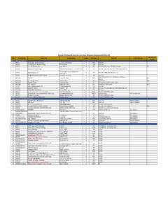
www.iiitd.ac.inIntroduction to 3D Production Design for Animation and Games Anoop Ratn(V) 4 I3D UG/PG 59 DES522 Inclusive Design, Universal Design & Accessibility(New) Richa Gupta 4 IDUDA UG/PG 60 ECE314/ECE514 Digital VLSI Design Anuj Grover 4 DVD UG/PG 61 ECE315/ECE515 Analog CMOS Design G.S. Visweswaran(V) 4 CMOS UG/PG

Memory in SystemVerilog
www.cs.columbia.edu0/1 0 Z: “not connected” 0 1 0 1 1 1 ... Introduction to CMOS VLSI Design. Addison-Wesley, 2010. Intel’s 2102 SRAM, 1024 1 bit, 1972. 2102 Block Diagram. SRAM Timing A12 A11 A2 A1 A0 CS2 D7 D6 D1 D0..... CS1 WE OE 6264 8K 8 SRAM CS1 CS2 WE OE Addr 1 …

アナログ集積回路の レイアウト技術
kobaweb.ei.st.gunma-u.ac.jpC. Mead and L. Conway, Introduction to VLSI Systems, Addison-Wesley, 1980. 6 アナログアナログ技術 技術シリーズ アナログアナログ集積回路 集積回路 ... 0=VSS VDD CMOS ...

Lecture 6: Logical Effort
user.engineering.uiowa.edu6: Logical Effort CMOS VLSI DesignCMOS VLSI Design 4th Ed. 4 Example Ben Bitdiddle is the memory designer for the Motoroil 68W86, an embedded automotive processor. Help Ben design the decoder for a register file. Decoder specifications: – 16 word register file – Each word is 32 bits wide – Each bit presents load of 3 unit-sized transistors
LECTURE NOTES ON VLSI DESIGN B.Tech VII semester (R16)
www.iare.ac.inCMOS processes were widely adopted and have essentially replaced nMOS and bipolar processes ... names would have to be created every five years if this naming trend continued and thus the term very large-scale integration (VLSI) is used to describe most integrated circuits from the 1980s onward. A corollary of ... Feature sizes down to 0.25 µm ...
Chapter 4 Low-Power VLSI DesignPower VLSI Design
www.ee.ncu.edu.tw4/4 1 0 t iti l k4/4 = 1.0 transition per clock • Gray-code counter is more power efficient.code counter is more power efficient. G. K. Yeap, Practical Low Power Digital VLSI Design, Boston: Kluwer Academic Publishers (now Springer) 1998 National Central University EE4012VLSI Design 30 Kluwer Academic Publishers (now Springer), 1998.

CHAPTER 8: Diffusion
www.cityu.edu.hk0 0 where S is the total amount of dopant per unit area. The solution of the diffusion equation satisfying the above conditions is: C x t S Dt x Dt ( , ) p 2 4 (Equation 8.8) This expression is the Gaussian distribution, and the dopant profile is displayed in Figure 8.4b. By substituting x = 0 into Equation 8.8: C t S s Dt ( ) (Equation 8.9)

Cadence Tutorial C: Simulating DC and Timing ...
www.egr.msu.eduo parameters vs=0 o vdd (vdd! 0) vsource dc=3 o Gnd (gnd! 0) vsource dc=0 o v1 (A 0) vsource dc=vs o dcs dc param=vs start=0 stop=3 step=0.01 This assumes your input node is called ‘A’. Note an output capacitance is not needed since we are doing a DC analysis and timing will not be considered. Instead a DC statement is needed.