Example: dental hygienist
CHAPTER 8: Diffusion
0 0 where S is the total amount of dopant per unit area. The solution of the diffusion equation satisfying the above conditions is: C x t S Dt x Dt ( , ) p 2 4 (Equation 8.8) This expression is the Gaussian distribution, and the dopant profile is displayed in Figure 8.4b. By substituting x = 0 into Equation 8.8: C t S s Dt ( ) (Equation 8.9)
Tags:
Information
Domain:
Source:
Link to this page:
Documents from same domain

Chow Yei Ching School of Graduate Studies
www.cityu.edu.hkCity University of Hong Kong | 2019 Entry Chow Yei Ching School of Graduate Studies City University of Hong Kong Tat Chee Avenue Kowloon Hong Kong

How to prepare for IELTS - City University of Hong …
www.cityu.edu.hkHow to prepare for IELTS Reading 1 Contents Page Details of the reading test 2 The Question Types 1. Multiple choice 4 2. Short answer questions 6
CITY UNIVERSITY OF HONG KONG
www.cityu.edu.hkCity University of Hong Kong Information on a Course ... EMSD (latest edition). Code of Practice for the Electricity (Wiring) Regulations. Electrical and Mechanical
City University of Hong Kong
www.cityu.edu.hkCity University of Hong Kong Information on a Course ... EMSD. 2000, Code of Practice on the Design and Construction of Lifts and Escalators, EMSD of HKSAR.

To wipe a mobile device remotely by Office 365 V2.1
www.cityu.edu.hkHow to wipe a mobile device remotely by Office 365 When your mobile device is lost or stolen, wipe the device remotely may be the last resort to protect the information from being disclosed to the others.
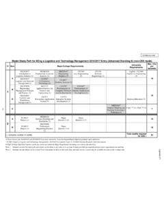
Model Study Path for BEng e-Logistics and …
www.cityu.edu.hkModel Study Path for BEng e-Logistics and Technology Management 2016/2017 Entry (Advanced Standing II) (non-CES mode) Yr . Sem Major/College Requirements

How to prepare for IELTS - City University of Hong …
www.cityu.edu.hkHow to prepare for IELTS Writing 2 Details of the Writing Test Procedure of the test The writing test is the third test you do on the test day. You have 60 minutes for this test.
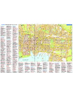
PALERMO Principali monumenti e palazzi PALERMO
www.cityu.edu.hkAB C D E F G H I L 1 1 2 2 3 3 4 4 5 5 6 6 7 7 AB C D E F G H I L G s V V G G G G G 7 30 5 6 16 60 18 92 97 61 93 98 96 82 25 9 22 14 73 65 T T T T T T T 55 95 63 2 3 8 5 7 2 26 49 32 64 T 72 57 Villa Giardino

The Common Recruitment Examination
www.cityu.edu.hk1 Format of the Common Recruitment Examination (CRE) The information below is taken from the HKSAR Government website. For more details on the CRE exam, such as the grade requirements and FAQs, go directly to
To wipe a mobile device remotely by Office 365 V2.1
www.cityu.edu.hkHow to wipe a mobile device remotely by Office 365 When your mobile device is lost or stolen, wipe the device remotely may be the last resort to protect the information from being disclosed to the others.
Related documents
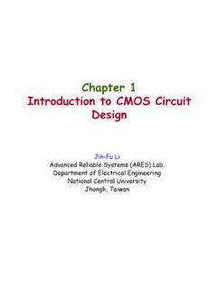
Chapter 1 Introduction to CMOS Circuit Design
www.ee.ncu.edu.twIntroduction to CMOS Circuit Design Jin-Fu Li Advanced Reliable Systems (ARES) Lab. ... A=0 Mn Off V DD V A V Tn 0 Logic translation V A V GSn Drain Mn Source Gate-source voltage Gate +-V A=1 Mp Off V A=0 Mp On V DD V A V ... Design Flow for a VLSI Chip Specification Behavioral Design Structural Design Physical Design Function Function Function ...
Course Offering UG 2nd Year and Rest, Monsoon Semester ...
www.iiitd.ac.inIntroduction to 3D Production Design for Animation and Games Anoop Ratn(V) 4 I3D UG/PG 59 DES522 Inclusive Design, Universal Design & Accessibility(New) Richa Gupta 4 IDUDA UG/PG 60 ECE314/ECE514 Digital VLSI Design Anuj Grover 4 DVD UG/PG 61 ECE315/ECE515 Analog CMOS Design G.S. Visweswaran(V) 4 CMOS UG/PG

Memory in SystemVerilog
www.cs.columbia.edu0/1 0 Z: “not connected” 0 1 0 1 1 1 ... Introduction to CMOS VLSI Design. Addison-Wesley, 2010. Intel’s 2102 SRAM, 1024 1 bit, 1972. 2102 Block Diagram. SRAM Timing A12 A11 A2 A1 A0 CS2 D7 D6 D1 D0..... CS1 WE OE 6264 8K 8 SRAM CS1 CS2 WE OE Addr 1 …

アナログ集積回路の レイアウト技術
kobaweb.ei.st.gunma-u.ac.jpC. Mead and L. Conway, Introduction to VLSI Systems, Addison-Wesley, 1980. 6 アナログアナログ技術 技術シリーズ アナログアナログ集積回路 集積回路 ... 0=VSS VDD CMOS ...

Lecture 6: Logical Effort
user.engineering.uiowa.edu6: Logical Effort CMOS VLSI DesignCMOS VLSI Design 4th Ed. 4 Example Ben Bitdiddle is the memory designer for the Motoroil 68W86, an embedded automotive processor. Help Ben design the decoder for a register file. Decoder specifications: – 16 word register file – Each word is 32 bits wide – Each bit presents load of 3 unit-sized transistors
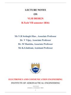
LECTURE NOTES ON VLSI DESIGN B.Tech VII semester (R16)
www.iare.ac.inCMOS processes were widely adopted and have essentially replaced nMOS and bipolar processes ... names would have to be created every five years if this naming trend continued and thus the term very large-scale integration (VLSI) is used to describe most integrated circuits from the 1980s onward. A corollary of ... Feature sizes down to 0.25 µm ...
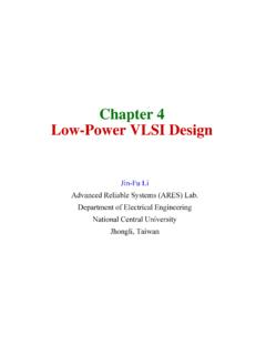
Chapter 4 Low-Power VLSI DesignPower VLSI Design
www.ee.ncu.edu.tw4/4 1 0 t iti l k4/4 = 1.0 transition per clock • Gray-code counter is more power efficient.code counter is more power efficient. G. K. Yeap, Practical Low Power Digital VLSI Design, Boston: Kluwer Academic Publishers (now Springer) 1998 National Central University EE4012VLSI Design 30 Kluwer Academic Publishers (now Springer), 1998.

Cadence Tutorial C: Simulating DC and Timing ...
www.egr.msu.eduo parameters vs=0 o vdd (vdd! 0) vsource dc=3 o Gnd (gnd! 0) vsource dc=0 o v1 (A 0) vsource dc=vs o dcs dc param=vs start=0 stop=3 step=0.01 This assumes your input node is called ‘A’. Note an output capacitance is not needed since we are doing a DC analysis and timing will not be considered. Instead a DC statement is needed.