Buck Boost
Found 7 free book(s)
LTC3335 - Nanopower Buck-Boost DC/DC with Integrated …
www.analog.comNanopower Buck-Boost DC/DC with Integrated Coulomb Counter The LTC®3335 is a high efficiency, low quiescent current (680nA) buck-boost DC/DC converter with an integrated precision coulomb counter which monitors accumulated battery discharge in long life battery powered applications. The buck-boost can operate down to 1.8V on its input and

POWER CONVERTER TOPOLOGY TRENDS - PSMA
www.psma.comBOOST BUCK-BOOST BUCK ACTIVE CLAMP 2-SWITCH LLC. Isolated Power Topology Derivatives 8 “Mainstream” Converter Topologies Non-Isolated 1. Boost 4. 2. Buck-Boost 5. 3. Buck 6. Isolated Flyback Forward Push-Pull 7. Half Bridge 8. Full Bridge. Power levels numbers for general . discussion only. Exceptions aplenty.
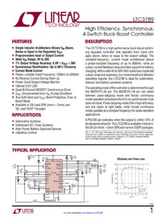
LTC3789 – High Efficiency, Synchronous, 4-Switch Buck-Boost …
www.analog.com4-Switch Buck-Boost Controller The LTC®3789 is a high performance buck-boost switch-ing regulator controller that operates from input volt-ages above, below or equal to the output voltage. The constant-frequency, current mode architecture allows a phase-lockable frequency of up to 600kHz, while an
Topologies for switch mode power supplies
www.st.comII.2 The “Boost” converter: Step up voltage regulator Figure 2 : The step up “Boost” regulator In normal operation, the energy is fed from the inductor to the load, and then stored in the output capacitor. For this reason, the output capacitor is stressed a lot more than in the Buck converter. V in 1-δ V out = ton T δ= Device ...
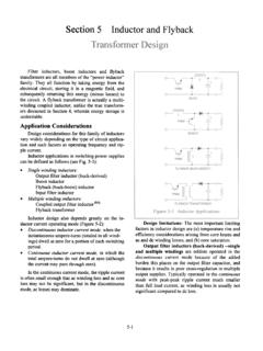
'Magnetics Design 5 - Inductor and Flyback Transformer …
www.ti.comBoost and input filter inductors and single winding flyback inductors are often designed to operate in the continuous mode. As with the buck-derived filter inductors described previously, inductor design is then usually limited by dc winding losses and core saturation. However, many boost and flyback applications
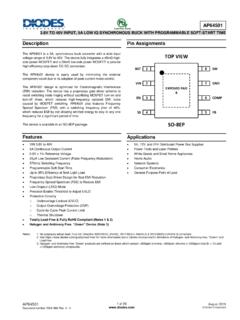
TOP VIEW - Diodes Incorporated
www.diodes.comThe AP64501 is a 5A, synchronous buck converter with a wide input voltage range of 3.8V to 40V. The device fully integrates a 45mΩ high- ... High-Side Gate Drive Boost Input. BST supplies the drive for the high-side N-Channel power MOSFET. A 100nF capacitor is recommended from BST to SW to power the high-side driver.
Snubber Circuits: Theory , Design and Application - TI.com
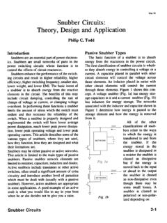
www.ti.comBUCK r l ~Do Lo ~I 4--Q I v, -~ BOOST-"Co RL ~Do Lo ~I-4---Q-=-v switch for a particular purpose. An inductor in series with the switch, a comnt snubber, presents the switch with an inductive load at turn-on so that it switches on with zero comnt. This is a modifi-cation of the load which would typically be some-what capacitive at turn-on.