Differential Driver
Found 8 free book(s)
MAX3483/MAX3485/MAX3486/MAX3488/MAX3490/MAX3491 …
datasheets.maximintegrated.comDifferential Driver Output VOD RL = 100Ω (RS-422), Figure 4 2.0 RL = 54Ω (RS-485), Figure 4 1.5 V RL = 60Ω (RS-485), VCC = 3.3V, Figure 5 1.5 Change in Magnitude of Driver Differential Output Voltage for Complementary Output States (Note 1) ΔVOD RL = 54Ω or 100Ω, Figure 4 0.2 V Driver Common-Mode Output Voltage VOC RL = 54Ω or 100Ω ...
Single-Reduction Differential Carriers - Parts Manuals
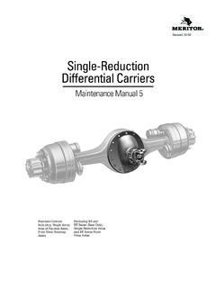
partsmanuals.orgDifferential Carriers Maintenance Manual 5 Revised 10-06 Standard Carriers Including: Single Axles, Rear of Tandem Axles, Front Drive Steering Axles Excluding RS and RT Series (Rear Only), ... Driver-Controlled Full Locking Main Differential T-9007V. $50. Order T …

AD8129/AD8130 Low Cost 270 MHz Differential Receiver ...
www.analog.commode and differential-mode voltage ranges while maintaining signal integrity. The wide common-mode voltage range enables the driver-receiver pair to operate without isolation transformers in many systems where the ground potential difference between drive and receive locations is many volts. The AD8129/AD8130

1. General description - NXP
www.nxp.comthe CANL driver is switched off and the RTL bias changes to the pull-up current source. Reception continues by switching to the single-wire mode via pins CANH or CANL. When failures 4 or 7 are removed, the recessive bus levels are restored. If the differential
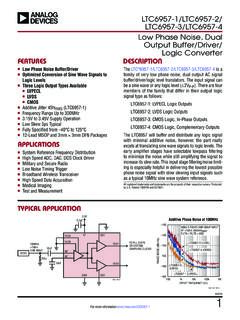
LTC6957-1/LTC6957-2/LTC6957-3/LTC6957-4 - Analog Devices
www.analog.comVINDIFF Input Signal Level Range, Differential l 0.2 0.8 2 VP-P tMIN Minimum Input Pulse Width High or Low 0.5 ns VINCM Self-Bias Voltage, IN+, IN– l 1.8 2 2.3 V RIN Input Resistance, Differential l 1.5 2 2.5 kΩ CIN Input Capacitance, Differential 0.5 pF BWIN ++ + LTC6957-2

Board Design Guidelines for PCI Express™ Architecture
e2e.ti.com§Clock driver requirements: ü100MHz with SSC support (e.g. CK410) üSystem board (source) termination only üRise/fall slew rate requirements need to be met System board requirements L1 L1' L2 L2' L3' L3 L5 L5' Rs Rs Rt Rt PCI Express 1” Connector Clock Driver PCI Express Card L4 L4' 0.5” max 0–0.2” 0 – 0.2” – 14” 0.5” – 3 ...
LM358 - Diodes Incorporated
www.diodes.comDifferential Input Voltage 32 V V IN Input Voltage -0.3 to +32 V P D Power Dissipation (Note 2) 600 mW Output Short-Circuit to GND (One Amplifier) (Note 3) V+ < 15V and T A=25 oC Continuous Input Current (V IN < -0.3V) (Note 4) 40 mA T OP Operating Temperature Range 0 to +70 oC T ST Storage Temperature Range -65 to +150 oC Notes: 2.
LM2596 - 3.0 A, Step-Down Switching Regulator
www.onsemi.comINPUT - OUTPUT DIFFERENTIAL (V) TJ, JUNCTION TEMPERATURE (°C) Figure 2. Normalized Output Voltage TJ, JUNCTION TEMPERATURE (°C) Figure 3. Line Regulation Figure 4. Dropout Voltage Figure 5. Current Limit Figure 6. Quiescent Current Figure 7. Standby Quiescent Current ILoad = 200 mA ILoad = 3.0 A Vin = 12 V Vin = 40 V L1 = 33 H Rind = 0.1 ...