Diode Schottky Diode
Found 7 free book(s)
LTC4353 - Dual Low Voltage Ideal Diode Controller
www.analog.comIdeal Diode Controller The LTC®4353 controls external N-channel MOSFETs to implement an ideal diode function. It replaces two high power Schottky diodes and their associated heat sinks, saving power and board area. The ideal diode function permits low loss power supply ORing and supply holdup applications.
LT3462 (Rev. A) - Analog Devices
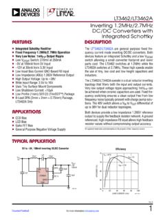
www.analog.comThe LT3462 has a built‑in Schottky diode. When supply voltage is applied to the VIN pin, the voltage difference between VIN and VD generates inrush current flowing from input through the inductor and the Schottky diode to charge the flying capacitor to V IN. The maximum non‑ repetitive surge current the Schottky diode in the LT3462

BLOCKING DIODE INSTALLATION INSTRUCTIONS - Marlec
www.marlec.co.ukIt is usual to fit the blocking diode into the positive output inside the terminal box of the solar module at the positive end of each series string. In order to minimise voltage drop and power loss it is recommended that Schottky diodes are used. Modules up to 60W 5A Schottky Diode Marlec Part No 913-005

Metal/Semiconductor Ohmic Contacts - Stanford University
web.stanford.educrude. An ohmic contact is generally modeled as a heavily doped Schottky (diode) contact. The Schottky model predicts that upon bringing in contact Si with electron affinity X, and a metal of work function φm, a barrier of height φb = (φm − χ) which is independent of semiconductor doping will be formed. Since measured φm values for a ...

Power MOSFET Selection Guide - NXP
www.nxp.comSchottky or Schottky-like diode but without problematic high leakage current. Efficiency is excellent, even at higher frequencies, making NextPowerS3 the perfect choice for high power density DC:DC applications. #1 for Hot-swap MOSFETs In applications such as hot-swap and soft-start, power MOSFETs are deliberately turned
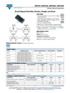
Small Signal Schottky Diodes, Single and Dual
www.vishay.comFig. 2 - Diode Capacitance vs. Reverse Voltage VR ELECTRICAL CHARACTERISTICS (Tamb = 25 °C, unless otherwise specified) PARAMETER TEST CONDITION SYMBOL MIN. TYP. MAX. UNIT Reserve breakdown voltage IR = 100 μA (pulsed) V(BR) 30 V Leakage current Pulsed test tp < 300 μs, δ <2 % at VR = 25 V IR 2μA Forward voltage

TYPICAL APPLICATION
atta.szlcsc.comNo Schottky Diode Required 4.5V to 16V Input Voltage Range 0.6V Reference GENERAL DESCRIPTIONSlope Compensated Current Mode Control for Excellent Line and Load Transient Response Integrated internal compensation Stable with Low ESR Ceramic Output Capacitors Over Current Protection with Hiccup-Mode