Substrate mapping and device
Found 8 free book(s)
STEP: E142 Substrate Mapping and Device Traceability ...
dom.semi.org8 STEP: E142 Substrate Mapping and Device Traceability - Introduction to the E142 Standard - Dave Huntley Participants • The SEMI E142 Substrate Mapping standard

Leakage Current in Sub-Micrometer CMOS Gates
inf.ufrgs.br6 Paulo Francisco Butzen and Renato Perez Ribas significantly leakage current through these drain- and source-to-substrate junctions under high reversed biasing [8]. These are the three major types of leakage mechanisms:

IPFA 2018 TECHNICAL PROGRAM 16 - 19 July
www.ipfa-ieee.orgTime 08:30 hrs 08:30 - 10:30 hrs TUT A1 BEOL Reliability - From FinFETs to More-than-Moore Devices (Dr. Jeff Gambino, ON Semiconductor , USA) TUT B1

Datasheet - L9907 - Automotive FET driver for 3 phase BLDC ...
www.st.comDescription L9907 6/45 DS11800 Rev 2 1 Description L9907 is a smart power device realized in STMicroelectronics advanced BCD-6s technology. It is able to drive all …

Scanning Surface Inspection System with Defect-review …
www.hitachi.comScanning Surface Inspection System with Defect-review SEM and Analysis System Solutions 78 Scanning Surface Inspection System with Defect-review
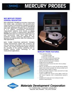
MDC MERCURY PROBES GENERAL DESCRIPTION
www.mdc4cv.comMDC MERCURY PROBES GENERAL DESCRIPTION MDC MERCURY PROBES are precision instruments that enable rapid, convenient, and non-destructive measurements of …
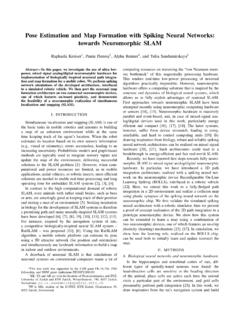
Pose Estimation and Map Formation with Spiking Neural ...
www.sandamirskaya.euFig. 3: Collision detection network: CD neurons are driven by 8 collision-sensors and represent the position of the colli-sion around the robot in an activity “bump”.
Embedded Wafer Level Ball Grid Array - STATS ChipPAC Ltd
www.statschippac.comwwwstatschippaccom Market Leader in Embedded FOWLP Technology A breakthrough technology, embedded Wafer Level Ball Grid Array (eWLB) is a versatile …